Xilinx ML310 User Manual
Page 39
ML310 User Guide
39
UG068 (v1.01) August 25, 2004
1-800-255-7778
Board Hardware
R
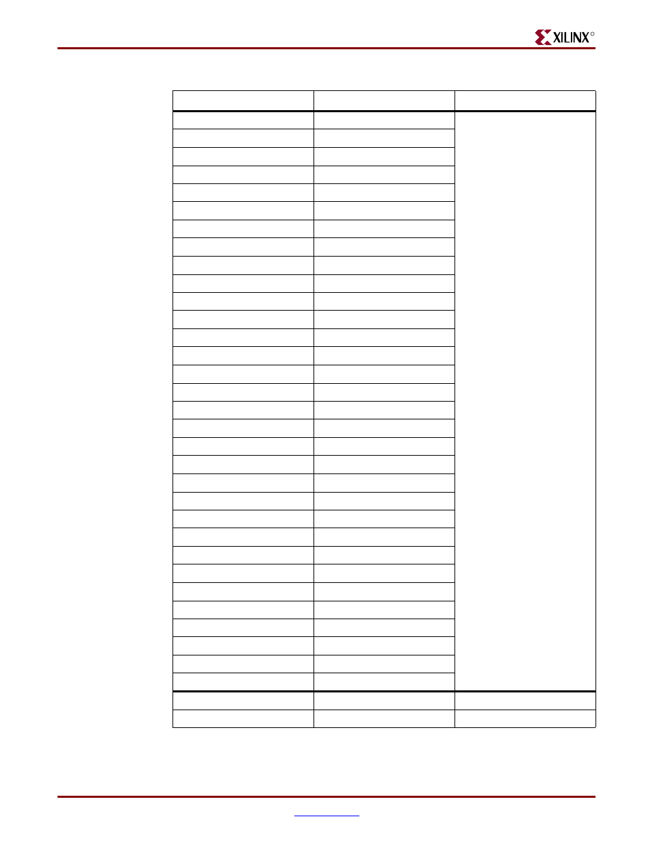
PCI_AD[0]
G5
PCI Address/Data Lines
PCI_AD[1]
G6
PCI_AD[2]
D5
PCI_AD[3]
C5
PCI_AD[4]
C1
PCI_AD[5]
C2
PCI_AD[6]
J7
PCI_AD[7]
J8
PCI_AD[8]
D3
PCI_AD[9]
C4
PCI_AD[10]
D1
PCI_AD[11]
D2
PCI_AD[12]
H5
PCI_AD[13]
H6
PCI_AD[14]
E3
PCI_AD[15]
E4
PCI_AD[16]
E1
PCI_AD[17]
E2
PCI_AD[18]
K7
PCI_AD[19]
K8
PCI_AD[20]
F3
PCI_AD[21]
F4
PCI_AD[22]
F1
PCI_AD[23]
F2
PCI_AD[24]
J5
PCI_AD[25]
J6
PCI_AD[26]
G3
PCI_AD[27]
G4
PCI_AD[28]
G1
PCI_AD[29]
G2
PCI_AD[30]
L7
PCI_AD[31]
L8
PCI_PAR
H3
PCI_P_PAR
PCI_RST_N
N8
PCI_P_RST_N
* Note:
These signals are connected, but are not required for 32 bit only PCI systems.
Table 2-10:
PCI Controller Connections (Continued)
UCF Signal Name
XC2VP30 Pin (U37)
Description