High-speed i/o – Xilinx ML310 User Manual
Page 61
ML310 User Guide
61
UG068 (v1.01) August 25, 2004
1-800-255-7778
High-Speed I/O
R
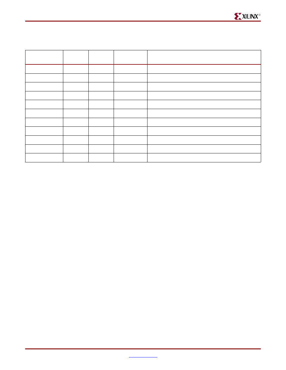
Shows the various Voltage monitor information.
High-Speed I/O
Xilinx Virtex-II Pro FPGAs offer a variety of high-speed I/O solutions. The ML310
Embedded Development Platform’s high-speed I/O is based on the XC2VP30-FF896
FPGA’s RocketIO multi-gigabit transceivers (MGTs) and LVDS capability. The high-speed
I/O signals on the FPGA are accessible through two personality module (PM) connectors,
PM1 and PM2, on the ML310 board. The ML310 is the host board, functioning as the
development platform for Virtex-II Pro FPGA. The PM connectors on the ML310 board
provide a means for extending the functionality of the board through high-speed I/O pins.
Personality modules connect to the ML310 board using Tyco Z-Dok+ docking connectors,
PM1 and PM2. In addition to having differential pairs and shielding ground connections,
Z-Dok+ connectors include utility connections for power, ground, and sensing. Tyco Z-
Dok+ high-speed connectors are rated to 6.25 Gb/s.
shows a personality module connected to the ML310 board through the PM1
and PM2 connectors. The plug, located on the ML310 board, is referred to as the host board
connector; the receptacle, located on the personality module, is referred to as the adapter
board connector.
Table 2-28:
Voltage Monitor Information
Schem Name
Voltage
Testpoint
*Indicator
LED
Notes
VCC1V5
1.5V
TP17
DS8
Regulated FPGA Core voltage
VCC2V5
2.5V
TP14
DS6
Regulated FPGA / Board Logic
VCC3_PCI
3.0V
TP10
DS4
Regulated FPGA PCI Bank 1-2 Voltage
VCC3V3
3.3V
TP8
DS2
Regulated PCI/Misc Logic
VCC5V
5.0V
TP16
DS7
From ATX Supply, All Regulators Derive Power
VTT_DDR
1.25V
TP13
DS5
Regulated DDR Termination (SSTL2)
MGT_AVCC
2.5V
N/A
DS3
Regulated MGT Power
MGT_VTT
1.8V
N/A
DS1
Regulated MGT Power
VCC3V3_ATX
3.3V
TP20
N/A
Not used
VCC12V_P
+12V
TP18
N/A
Direct from ATX Supply
VCC12V_N
-12V
TP19
N/A
Direct from ATX Supply
* Green = Voltage Nominal
* Red = Voltage Fault