8 oscillator divider 1 register (oscdiv1), Oscdiv1), Descriptions – Texas Instruments TMS320C642x DSP User Manual
Page 26: Section 2.4.8
www.ti.com
2.4.8
Oscillator Divider 1 Register (OSCDIV1)
PLL Controller
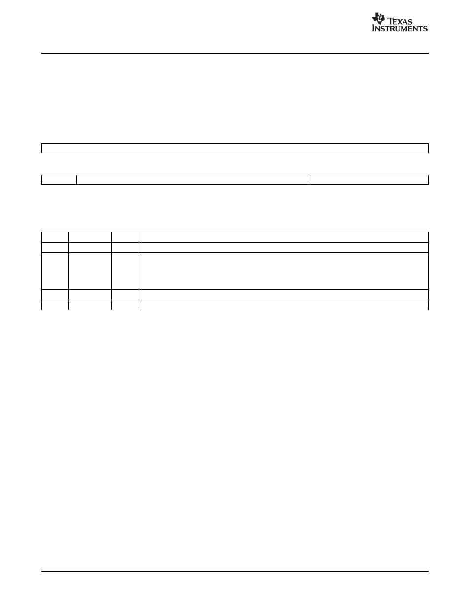
The oscillator divider 1 register (OSCDIV1) is shown in
and described in
. The oscillator
divider 1 controls divider for OBSCLK, dividing down from the MXI/CLKIN clock. For PLLC1, the OBSCLK
is connected to CLKOUT0 pin. OSCDIV1 only applies to PLLC1, and should not be used on PLLC2.
Figure 11. Oscillator Divider 1 Register (OSCDIV1)
31
16
Reserved
R-0
15
14
5
4
0
OD1EN
Reserved
RATIO
R/W-1
R-0
R/W-0
LEGEND: R/W = Read/Write; R = Read only; -n = value after reset
Table 17. Oscillator Divider 1 Register (OSCDIV1) Field Descriptions
Bit
Field
Value
Description
31-16
Reserved
0
Reserved
15
OD1EN
Oscillator divider 1 enable.
0
Oscillator divider 1 is disabled.
1
Oscillator divider 1 is enabled. For OBSCLK to toggle, both the OD1EN bit and the OBSEN bit in the
clock enable control register (CKEN) must be set to 1.
14-5
Reserved
0
Reserved
4-0
RATIO
0-1Fh
Divider ratio. Divider value = RATIO + 1. For example, RATIO = 0 means divide by 1.
26
Phase-Locked Loop Controller (PLLC)
SPRUES0B – December 2007