2 pll1 control – Texas Instruments TMS320C642x DSP User Manual
Page 12
www.ti.com
2.2
PLL1 Control
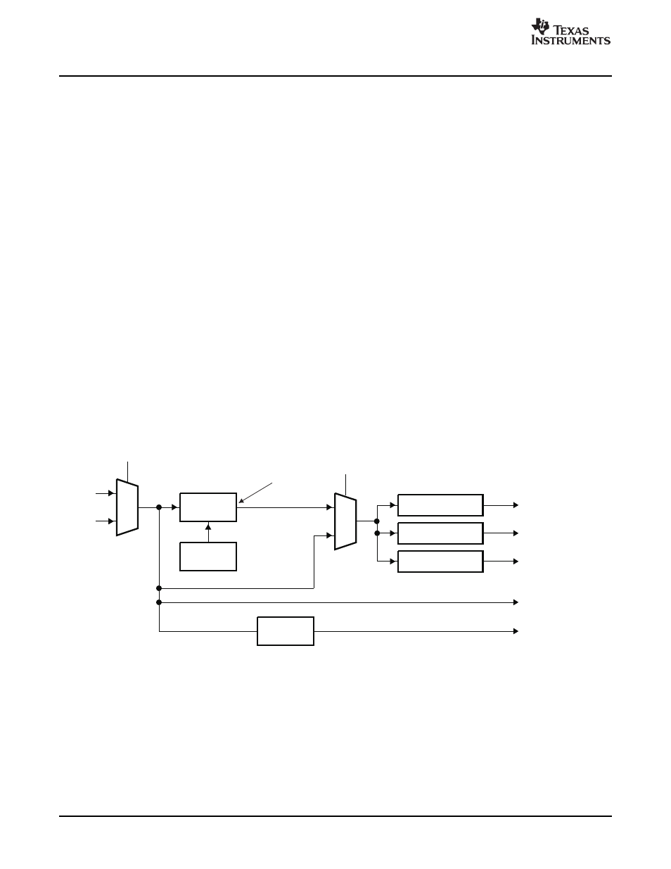
PLLDIV1 (/1)
PLLDIV3 (/6)
PLLDIV2 (/3)
SYSCLK1
(CLKDIV1 Domain)
SYSCLK3
(CLKDIV6 Domain)
SYSCLK2
(CLKDIV3 Domain)
1
0
PLLM
PLL
0
1
CLKMODE
CLKIN
OSCIN
PLLEN
AUXCLK
(CLKIN Domain)
OSCDIV1
OBSCLK
(CLKOUT0 Pin)
PLLOUT
PLL Controller
PLL1 supplies the primary C642x DSP system clock. Software controls the PLL1 operation through the
system PLL controller 1 (PLLC1) registers. The registers used in PLLC1 are listed in
shows the customization of PLL1 in the C642x DSP. The domain clocks are distributed to the core clock
domains (discussed in
) and the rest of the device as follows:
•
SYSCLK1: CLKDIV1 Domain
•
SYSCLK2: CLKDIV3 Domain
•
SYSCLK3: CLKDIV6 Domain
•
AUXCLK: CLKIN Domain
•
OBSCLK: CLKOUT0 pin
The PLL1 multiplier is controlled by the PLLM bit of the PLL multiplier control register (PLLM). The PLL1
output clock may be divided-down for slower device operation using the PLLC1 SYSCLK dividers
PLLDIV1, PLLDIV2, and PLLDIV3.
You are responsible to adhere to the PLLC1 frequency ranges and multiplier/divider ratios specified in the
data manual. See also
and
At power-up, PLL1 is powered-down and disabled, and must be powered-up by software through the PLL1
PLLPWRDN bit in the PLL control register (PLLCTL). By default, the system operates in bypass mode and
the system clock is provided directly from the input reference clock (MXI/CLKIN pin). Once the PLL is
powered-up and locked, software can switch the device to PLL mode operation by setting the PLLEN bit in
PLLCTL to 1. If the boot mode of the device is set to fast boot (FASTBOOT = 1), the bootloader code in
the Boot ROM will follow the previous process to power-up and lock the PLL, and switch the device to PLL
mode to speed up the boot process. Therefore, coming out of a fast boot, the device is operating in PLL
mode.
Figure 2. PLL1 Structure in the TMS320C642x DSP
12
Phase-Locked Loop Controller (PLLC)
SPRUES0B – December 2007