3 pll2 control – Texas Instruments TMS320C642x DSP User Manual
Page 16
www.ti.com
2.3
PLL2 Control
PLLDIV1 (/2)
1
0
PLLM
PLL
0
1
BPDIV
CLKMODE
CLKIN
OSCIN
PLLEN
PLL2_SYSCLK1
(DDR2 PHY)
PLL2_SYSCLKBP
(DDR2 VTP)
PLLOUT
PLL Controller
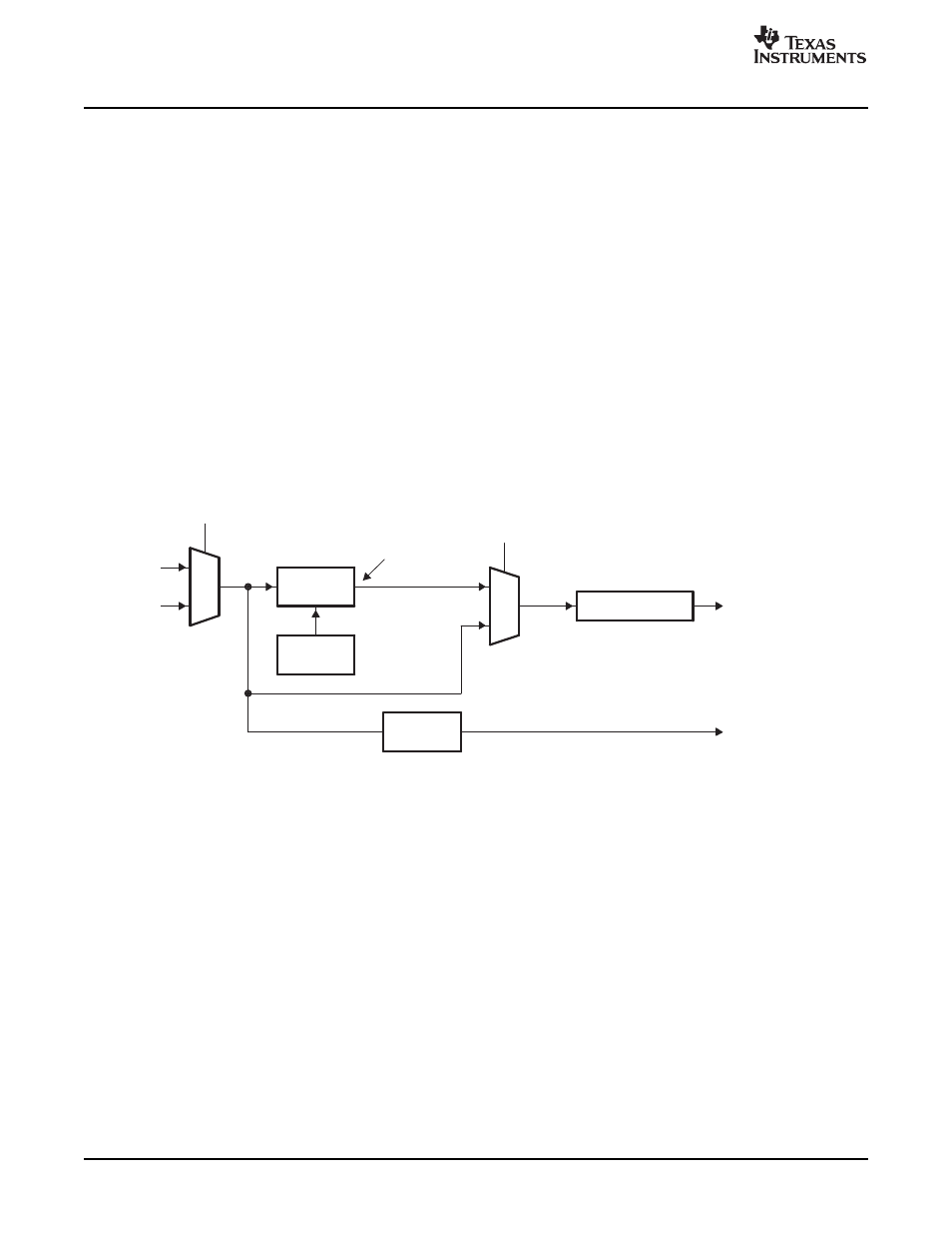
PLL2 provides the clock from which the DDR2 memory controller clocks are derived. The DDR PLL
controller 2 (PLLC2) controls PLL2, which accepts the clock from the oscillator and also generates the
various frequency clocks needed.
shows the customization of PLL2 in the C642x DSP. The PLL2
clocks are distributed to the device as follows:
•
SYSCLK1: DDR2 PHY
•
SYSCLKBP: DDR2 VTP
PLL2 supplies the DDR2 memory controller clock. Software controls the PLL2 operation through the DDR
PLL controller 2 (PLLC2) registers. The registers used in PLLC2 are listed in
. The PLL2
multiplier is controlled by the PLLM bit of the PLL multiplier control register (PLLM). The PLL2 multiplier
may be modified by software (for example, to tune the DDR interface for best performance).
The PLL2 output clock must be divided-down to the DDR operating range using the SYSCLK1 divider.
At power-up, PLL2 is powered-down and disabled, and must be powered-up by software through the PLL2
PLLPWRDN bit in the PLL control register (PLLCTL). By default, the system operates in bypass mode and
the DDR clock is provided directly from the input reference clock. Once the PLL is powered-up and locked,
software can switch the device to PLL mode operation by setting the PLLEN bit in PLLCTL to 1.
Figure 3. PLL2 Structure in the TMS320C642x DSP
16
Phase-Locked Loop Controller (PLLC)
SPRUES0B – December 2007