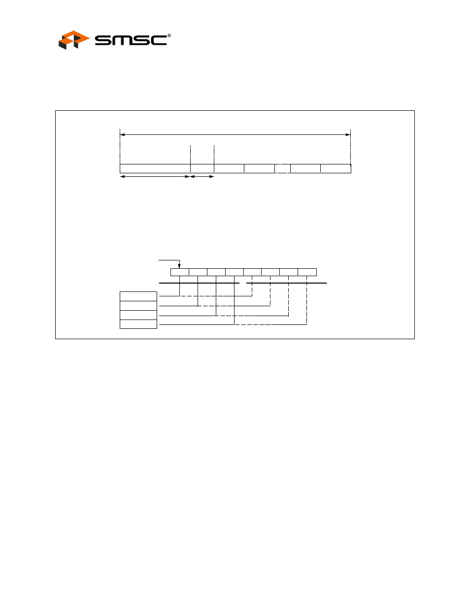
4 mii packet data communication with external phy, Figure 7.2 mii frame format & mii nibble order, Mii packet data communication with external phy – SMSC LAN91C111 User Manual
Page 24

10/100 Non-PCI Ethernet Single Chip MAC + PHY
Datasheet
Revision 1.91 (08-18-08)
24
SMSC LAN91C111 REV C
DATASHEET
7.5.4
MII Packet Data Communication with External PHY
The MIl is a nibble wide packet data interface defined in IEEE 802.3. The LAN91C111 meets all the
MIl requirements outlined in IEEE 802.3 and shown in
The Mll consists of the following signals: four transmit data bits (TXD[3:0]), transmit clock
(TX25),transmit enable (TXEN100), four receive data bits(RXD[3:0]), receive clock(RX25), carrier
sense (CRS100), receive data valid (RX_DV), receive data error (RX_ER), and collision (COL100).
Transmit data is clocked out using the TX25 clock input, while receive data is clocked in using RX25. The
transmit and receive clocks operate at 25 MHz in 100Mbps mode and 2.5 MHz in 10Mbps.
In 100 Mbps mode, the LAN91C111 provides the following interface signals to the PHY:
For transmission: TXEN100, TXD0-3, TX25
For reception: RX_DV, RX_ER, RXD0-3, RX25
For CSMA/CD state machines: CRS100, COL100
A transmission begins by TXEN100 going active (high), and TXD0-TXD3 having the first valid
preamble nibble. TXD0 carries the least significant bit of the nibble (that is the one that would go first
out of the EPH at 100 Mbps), while TXD3 carries the most significant bit of the nibble. TXEN100 and
TXD0-TXD3 are clocked by the LAN91C111 using TX25 rising edges. TXEN100 goes inactive at the
end of the packet on the last nibble of the CRC.
During a transmission, COL100 might become active to indicate a collision. COL100 is asynchronous
to the LAN91C111’s clocks and will be synchronized internally to TX25.
Reception begins when RX_DV (receive data valid) is asserted. A preamble pattern or flag octet will
be present at RXD0-RXD3 when RX_DV is activated. The LAN91C111 requires no training sequence
beyond a full flag octet for reception. RX_DV as well as RXD0-RXD3 are sampled on RX25 rising
Figure 7.2 MII Frame Format & MII Nibble Order
IDLE
PREAMBLE
PRMBLE
SFD
DATA 1
DATA N-1
DATA N
START
OF
FRAME
DELIM.
62 BT
DATA 2
DATA NIBBLES
2 BT
IDLE
TX_EN = 0
TX_EN = 0
TX_EN = 1
FIRST
NIBBLE
FIRST BIT
MAC's SERIAL BIT STREAM
D0
D1
D2
D3
D4
D5
D6
D7
TXD0 / RXD0
TXD3 / RXD3
TXD2 / RXD2
TXD1 / RXD1
MSB
SECOND
NIBBLE
MII
NIBBLE
STREAM
LSB
= [ BETWEEN 64-1518 DATA BYTES ]
= [ 1 1 ]
= [ 1 0 1 0 ... ] 62 BITS LONG
IDLE = TX_EN = 0
DATAn
SFD
PREAMBLE
