Intel 440GX User Manual
Page 94
Intel
®
440GX AGPset Design Guide
3-34
Design Checklist
•
Analog inputs feed inverting op-amp stages, useful for monitoring power supply regulation.
•
The LM79 is a 5V part, however SMBus requires a 3.3V interface. Level translation circuitry
is required. See the reference schematics for an example circuit.
•
CHASSIS_INTRU and FAN3 are pulled down and SMI_IN# is pulled up with 10K ohm
resistors.
•
The LM79 is connected to a programmable chip select on the PIIX4E. This assumes that the
LM79 is tied to the X-Bus. See PIIX4 Datasheet for more details.
3.18.3
82558B LOM Checklist
•
Refer to Application Note # 383, Intel 82558 LAN on Motherboard Design Guide, for
recommended PHY conformance testing (i.e., IEEE testing) and additional LOM design
details.
•
The PWR_GOOD circuitry (shown in Ap-Note 383) should be implemented if the power
supply dose not provide this signal.
•
Additional logic is needed to ensure that at least 4 clock cycles occur between ALTRST# and
ISOLATE# assertion.
•
The distance between “Magnetics” (i.e., Cat-3 or Cat-5 wire) and RJ-45 connector should be
kept to less than one inch.
•
Symmetrical 100 ohm traces should be used (differential impedance) for TDP/TDN and RDP/
RDN.
•
The 82558 requires decoupling on the power pins. At minimum, 3 capacitors
(2 x 0.1uF and 1 x 4.7uF) should be implemented on each side.
•
High speed traces between the 82558 to magnetic or magnetic to RJ45 should be routed
between layers to protect from EMI.
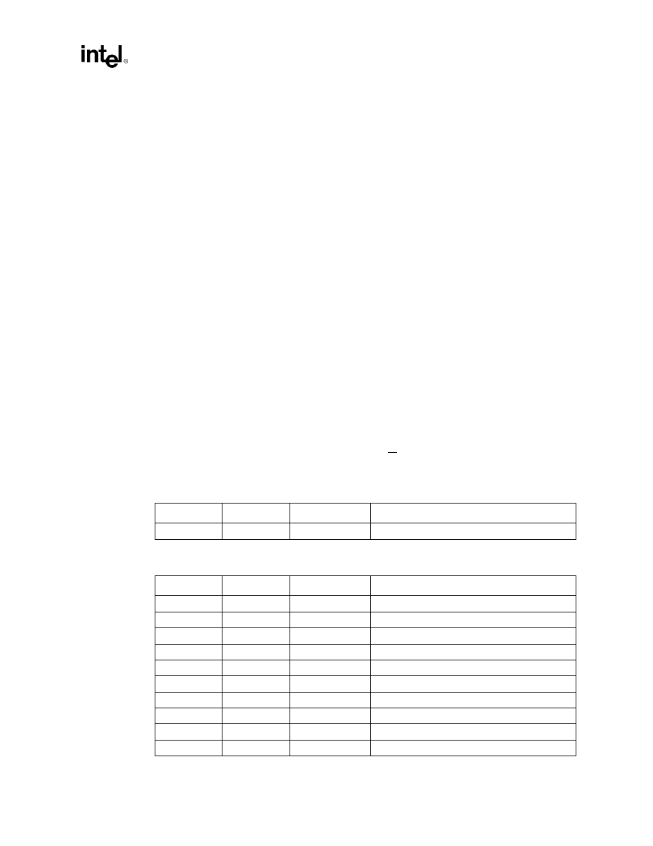
Pull-up resistors and values are recommended for the following pins:
Pull-down resistors and values are recommended for the following pins:
Pin Number
Pin Name
Resistor Value
Comment
15
ZREF
10K (5%)
Required in both A and B stepping designs
Pin Number
Pin Name
Resistor Value
Comment
30
TEST
1K (5%)
153
FLD4
10K (5%)
Not required for B-stepping designs
154
FLD3
10K (5%)
Not required for B-stepping designs
171
RDP
49.9 (1%)
172
RDN
49.9 (1%)
180
V
REF
220 (5%)
181
RBIAS10
768 (1%)
182
RBIAS100
634 (1%)
187
TDN
49.9 (1%)
204
AUXPWR#
220 (5%)