8 pci bus signals, 3 piix4e power and ground pins – Intel 440GX User Manual
Page 82
Intel
®
440GX AGPset Design Guide
3-22
Design Checklist
3.7.3
PIIX4E Power And Ground Pins
•
Vcc, Vcc(RTC), Vcc(SUS), and Vcc(USB) must be tied to 3.3V.
•
V
REF
must be tied to 5V in a 5V tolerant system. This signal must be power up before or
simultaneous to Vcc, and it must be power down after or simultaneous to Vcc. For the layout
guidelines, refer to the Pin Description section of the PIIX4E datasheet. The V
REF
circuitry
can be shared between 82443GX and the PIIX4E. If the circuitry is placed close to the PIIX4E,
then ensure that an extra 1uF capacitor is placed on the V
REF
pin of the 82443GX.
— STR support: For systems implementing STR support, a separate V
REF
circuit must be
used for each of the two devices since the PIIX4E Core and the 82443GX Host Bridge
should be supplied by the different power planes.
— No STR support: The V
REF
circuitry can be shared between 82443GX and the PIIX4E. If
the circuitry is placed close to the PIIX4E, then ensure that an extra 1uF capacitor is
placed on the V
REF
pin of the 82443GX.
•
Use a Schottky diode in the V
REF
circuit for a minimum voltage drop from VCC
3.3
to V
REF
because there is an internal diode in parallel to the Schottky diode that does not have high
current capability. The Schottky diode will begin to conduct first, therefore carrying the high
current.
•
V
REF
can be tied to Vcc in a non-5V tolerant system.
•
Tie Vss and Vss(USB) to ground.
3.8
PCI Bus Signals
A specific board sensitivity has been identified that may result in a low going glitch on a deasserted
PCIRST# signal when it is lightly loaded. This glitch may occur as a result of VCC droop caused
by simultaneous switching of most/all AD[31:0] signals from 0 to 1. This glitch can in some
designs be low enough (below 1.7V) to interfere with proper operation of the Host PCI Bridge
Controller component.
This sensitivity manifests itself on designs where PCIRST# is lightly loaded with less than
approximately 50pF, or is not driving the entire PCI bus. Design features that could aggravate the
problem are; an in-line active component on the PCIRST# signal, such as an AND gate or, lack of a
series termination resistor on the PCIRST# signal at the PIIX4 or PIIX4E.
There are several improvements that can be implemented individually or in any combination. First,
a series termination resistor between 22 and 33 ohms placed close to the PIIX4/PIIX4E will help
reduce the glitch. Second, an external capacitor of approximately 47pF will help reduce the glitch.
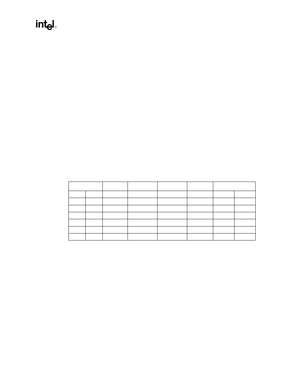
Table 3-9. PIIX4E PWR & GND
VCC
VCC(RTC)
VCC(SUS)
VCC(USB)
VSS(USB)
VSS
E9
F15
L16
N16
K5
J5
D10
L9-L12
E11
G6
R16
E7
M9-M12
E12
P15
E13
E16
R6
J9-J12
F5
R7
K9-K12
F6
R15
F14
T6