7 timing analysis – Intel 440GX User Manual
Page 41
Intel
®
440GX AGPset Design Guide
2-17
Motherboard Layout and Routing Guidelines
2.7
Timing Analysis
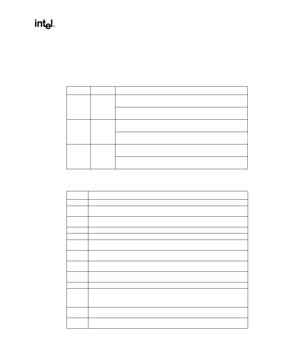
To determine the available flight time window perform an initial timing analysis. Analysis of setup
and hold conditions will determine the minimum and maximum flight time bounds for the host bus.
Use the following equations to establish the system flight time limits.
The terms used in the equations are described in
Table 2-8
.
Table 2-7. Intel
®
Pentium
®
II
Processor and Inte
®
l 440GX AGPset System Timing Equations
Driver
Receiver
Equation
Pentium
®
II
processor
AGPset
AGPset
Pentium
®
II
processor
Pentium
®
II
processor
Pentium
®
II
processor
T
T
T
T
T
T
flight
hold
co
skew CLK
skew PCB
clk
,min
,min
,
,
,max
≥
−
+
+
+
T
T
T
T
T
T
T
T
T
flight
cycle
co
su
skew CLK
skew PCB
jit
adj
clk
,max
,max
,
,
,min
≤
−
−
−
−
−
−
+
T
T
T
T
T
T
flight
hold
co
skew CLK
skew PCB
clk
,min
,min
,
,
,min
≥
−
+
+
−
T
T
T
T
T
T
T
T
T
flight
cycle
co
su
skew CLK
skew PCB
jit
adj
clk
,max
,max
,
,
,max
≤
−
−
−
−
−
−
−
T
T
T
T
T
flight
hold
co
skew CLK
skew PCB
,min
,min
,
,
≥
−
+
+
T
T
T
T
T
T
T
T
flight
cycle
co
su
skew CLK
skew PCB
jit
adj
,max
,max
,
,
≤
−
−
−
−
−
−
Table 2-8. Intel
®
Pentium
®
II
Processor and Intel
®
440GX AGPset System Timing Terms
Term
Description
T
cycle
System cycle time. Defined as the reciprocal of the frequency
T
flight,min
Minimum system flight time. Flight time is defined in
Section 4, “Debug Recommendations” on
page 4-1
.
T
flight,max
Maximum system flight time. Flight time is defined in
Section 4, “Debug Recommendations” on
page 4-1
.
T
co,max
Maximum driver delay from input clock to output data.
T
co,min
Minimum driver delay from input clock to output data.
T
su
Minimum setup time. Defined as the time for which the input data must be valid prior to the input
clock.
T
h
Minimum hold time. Defined as the time for which the input data must remain valid after the input
clock.
T
skew,CLK
Clock generator skew. Defined as the maximum delay variation between output clock signals
from the system clock generator.
T
skew,PCB
PCB skew. Defined as the maximum delay variation between clock signals due to system board
variation and Intel
®
440GX AGPset loading variation.
T
jit
Clock jitter. Defined as the maximum edge to edge variation in a given clock signal.
T
adj
Multi-bit timing adjustment factor. This term accounts for the additional delay that occurs in the
network when multiple data bits switch in the same cycle. The adjustment factor includes such
mechanisms as package and PCB crosstalk, high inductance current return paths, and
simultaneous switching noise.
T
clk,min
Minimum clock substrate delay. Defined as the minimum adjustment factor that accounts for the
delay of the clock trace on the Pentium II processor substrate.
T
clk,max
Minimum clock substrate delay. Defined as the maximum adjustment factor that accounts for the
delay of the clock trace on the Pentium II processor substrate.