1 matching the reference planes, 2 adding additional decoupling capacitor – Intel 440GX User Manual
Page 47
Intel
®
440GX AGPset Design Guide
2-23
Motherboard Layout and Routing Guidelines
There are also “population” rules which need to be observed. To properly adjust memory timings
for 100 MHz operation, it is asked of the OEM and end user to populate the motherboard starting
with the DIMM located the furthest from the 82443GX.
2.9.1.1
Matching the Reference Planes
Providing a good return path for the AC currents induced on the power and ground planes is critical
to reducing signal noise. The best way to provide a low inductance return path is to “match” the
BGA and motherboard reference planes for a given signal. For example, MD0 is routed on the
BGA next to the ground plane. To “match” the reference planes, MD0 should be routed on the
Motherboard such that it is closest to the motherboard ground plane. Routing the memory signals
in this manner will provide the best possible path for the return currents.
2.9.1.2
Adding Additional Decoupling Capacitor
Another way to provide a low inductance path for return currents is to provide additional
decoupling capacitors next to signal vias. It is not possible to route all the MD lines on a single
layer. As a result, some of the MD lines will transition between signal layers through vias. The
return currents associated with these signals also require a low inductance path between Vcc and
ground. This low inductance path is provided by decoupling capacitors between Vcc and ground.
These decoupling capacitors should be placed as close as possible to the signal vias.
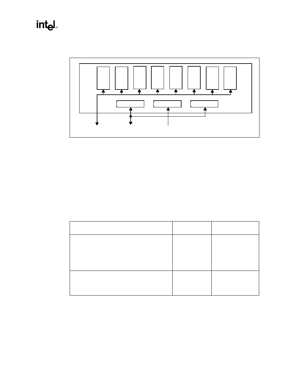
Figure 2-17. Registered SDRAM DIMM Example
SDR
A
M
SDR
A
M
S
DRAM
S
DRAM
S
DRAM
S
DRAM
SDR
A
M
SDR
A
M
Register
PLL
Register
Data
Control
Clock
Table 2-17. MDx lines Reference Planes Routing
Memory Data Line
82443GX BGA
Reference Layer
Motherboard
Reference Plane
MD0,MD1,MD2,MD3, MD4, MD7, MD11, MD14,
MD15, MD16, MD17, MD19, MD20, MD21, MD22,
MD23, MD27, MD28, MD29, MD31, MD33, MD36,
MD37, MD38, MD40, MD41, MD42, MD43, MD 44,
MD45, MD48, MD49, MD52, MD53,MD55, MD56,
MD 57, MD 58, MD61, MD62, MD63, MECC[6:0]
GND layer
GND plane
MD5, MD6, MD8, MD9, MD10, MD12, MD13, MD18,
MD24, MD25, MD26, MD30, MD32, MD34, MD35,
MD39, MD46, MD47, MD50, MD51, MD54, MD59,
MD60, MECC7
3.3v VCC layer
3.3v power plane