Intel 440GX User Manual
Page 86
Intel
®
440GX AGPset Design Guide
3-26
Design Checklist
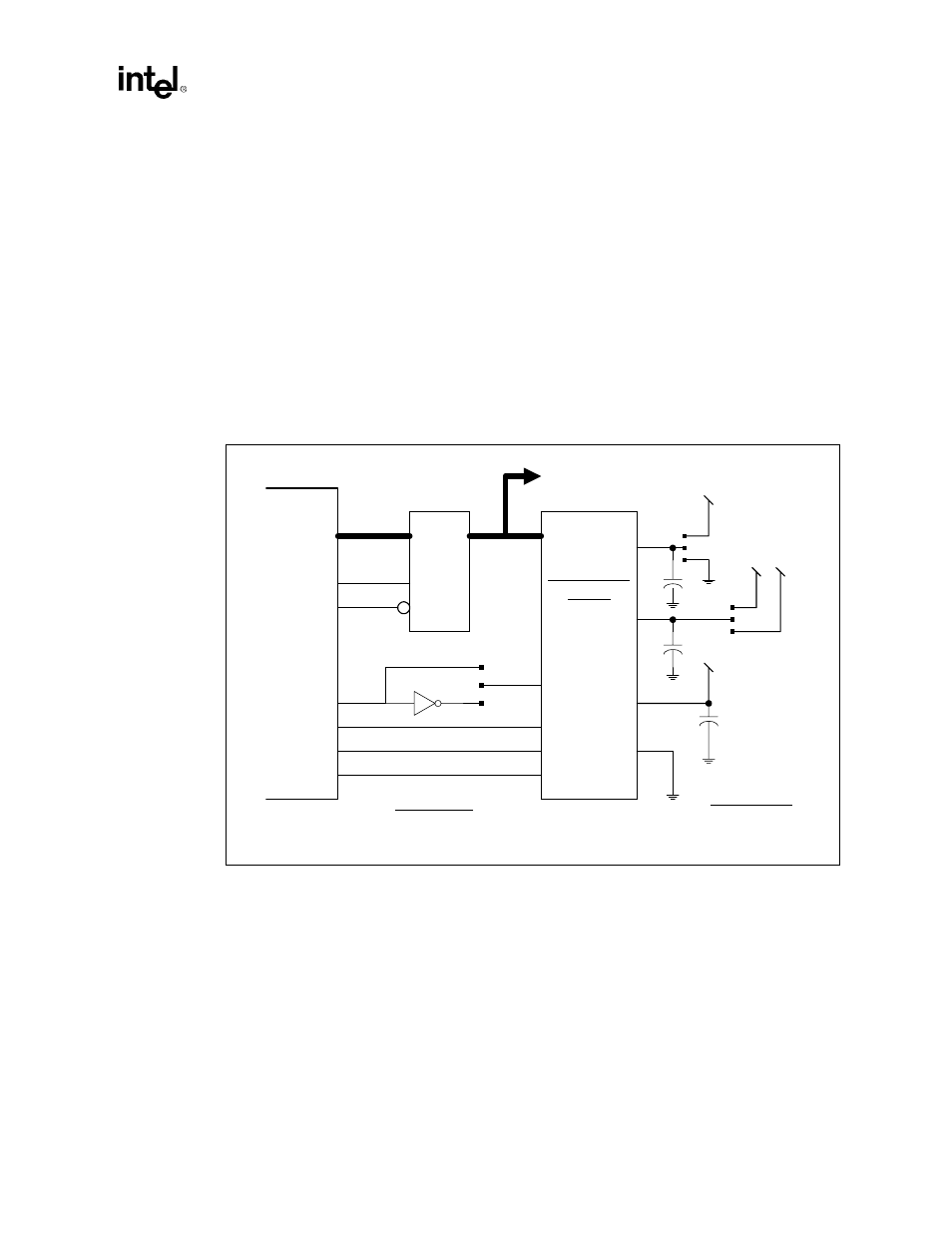
Following are general layout guidelines for using the Intel’s boot block flash memories
(28F001GX/28F002BC) in the system:
•
If adding a switch on VPP for write protection, switch to GND instead of VCC.
•
Connect the DU pin of the 2Mbit devices to GND if anticipating to use the Intel SmartVoltage
boot block flash memory family in the future.
•
Use A16 inversion for 1Mbit devices and A17 inversion for 2Mbit devices to differentiate
between recovery and normal modes. For systems needing a 1Mb to 2Mb upgrade path, A16
can be used for both devices alleviating the need for a board redesign.
•
Use a 0.01mf - 0.1mf ceramic capacitor connected between each Vcc and GND, and between
its Vpp and GND. These high frequency, inherently low inductance capacitors should be
placed as close as possible to the package leads.
Figure 3-6
illustrates the recommended layout for using Intel’s flash devices in desktop designs.
Simplified 2.7/3V/5V Design Considerations
Following are general layout guidelines for the Intel’s SmartVoltage/Smart 5 boot block flash
memory (2/4Mbit BV/B5) in 3V or 5V designs:
•
Connect 2.7V, 3V or 5V to V
CC
and connect 5V or 12V to V
PP
(program/erase levels) for BV
devices.
•
Connect 5V only to V
CC
and connect 5V or 12V to V
PP
(program/erase levels) for B5 devices.
•
If adding a switch on VPP for write protection, switch to GND instead of VCC.
•
Connect WP# to V
CC
, GND, or a general purpose output GPO[x] control signal. This pin
should not be left floating. WP# pin replaces a DU pin and is used in conjunction with the V
PP
and RP# pins, as detailed in the table below, to control write protection of the boot block.
Figure 3-6. nterfacing Intel’s Flash with PIIX4E in Desktop
0.01uf
0.01uf
SD[7:0]
X D I R #
X O E #
XD[7:0]
D I R
G
L S 2 4 5
A
B
S A 1 6 /
S A 1 7
M E M W #
M E M R #
B I O S C S #
V p p
R P #
V c c
D U
V c c
+ 1 2 V
+ 1 2 V
V c c
C E #
O E #
W E #
S A 1 6 /
S A 1 7
1
2
3
1
2
3
1
2
3
1 M b i t u s e s S A 1 6
2 M b i t u s e s S A 1 7
J1
J2
J3
1Mbit/2Mbit
Flash
Mode J1 J2
Program 1-2 1-2
PnP 1-2 2-3
Non-PnP 2-3 x
J 3
Mode POS
Recovery 1-2
Normal 2-3
PIIX4
PIIX4E