2 board description – Intel 440GX User Manual
Page 27
Intel
®
440GX AGPset Design Guide
2-3
Motherboard Layout and Routing Guidelines
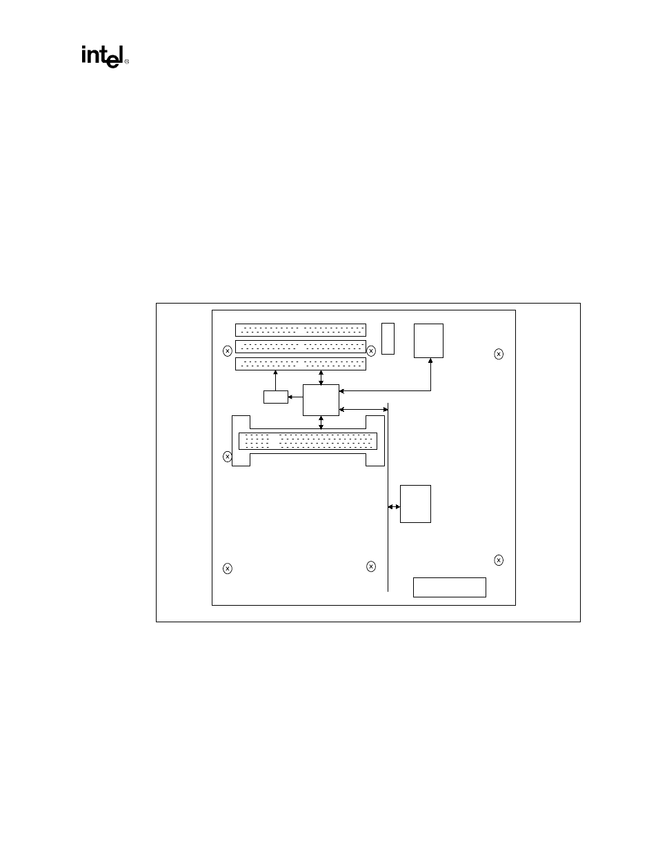
NLX Form Factor:
1. The NLX placement and layout below is recommended for a single (UP) Intel
®
Pentium
®
II
processor / Intel
®
440GX AGPset system design.
2. The example placement below shows one Slot 1 connector, 4 DIMM sockets, and an AGP
compliant device down.
3. For an NLX form factor design, the AGP compliant graphics device may readily be integrated
on the motherboard (device down option).
4. The trace length limitation between critical connections will be addressed later in this
document.
5.
Figure 2-3
is for reference only and the trade-off between the number of DIMM sockets, and
other motherboard peripherals need to be evaluated for each design.
2.2
Board Description
For a single processor / Intel
®
440GX AGPset motherboard design, a 4 layer stack-up arrangement
is recommended. The stack up of the board is shown in
Figure 2-4
. The impedance of all the signal
layers are to be between 50 and 80 ohms. Lower trace impedance will reduce signal edge rates,
over & undershoot, and have less cross-talk than higher trace impedance. Higher trace impedance
will increase edge rates and may slightly decrease signal flight times.
Figure 2-3. Example NLX Placement for a UP Intel
®
Pentium
®
II
processor / Intel
®
440GX
Design
82443GX
PIIX4E
AGP
Pentium
®
II
Slot 1
I/O Ports
SDRAM DIMMs
PCI0/ISA Riser
CK100
C K B F
v 0 0 3
Host Interface
PCI Interface
AGP Interface
S D R A M
Interface