11 divisor latch registers (dlm and dll), 2 16c550a uart fifo operation, 1 fifo interrupt mode operation – Intel MD566X User Manual
Page 127
56K V.92 Data, Fax, and Voice Chipset
Programmer’s Guide
Intel Confidential
127
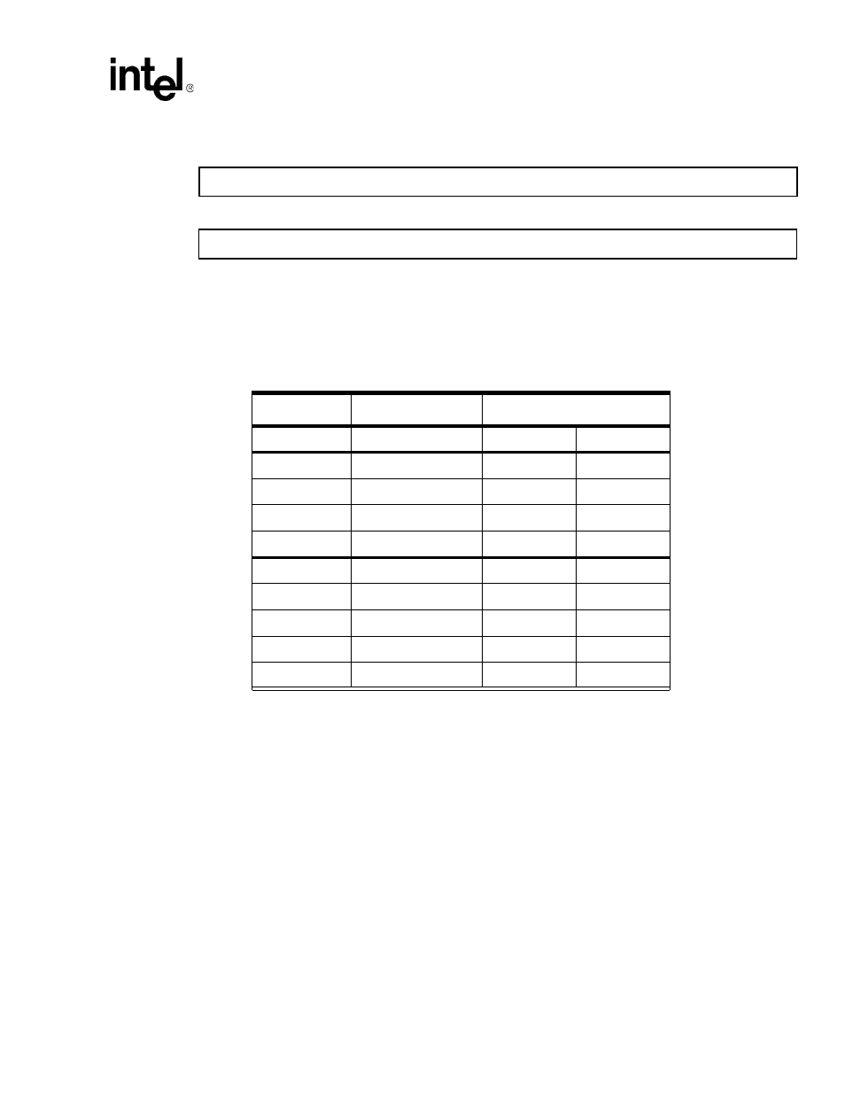
10.1.11Divisor Latch Registers (DLM and DLL)
The LS divisor latch (least-significant byte) and MS divisor latch (most-significant byte) are two read/write registers used to set
the modem data rate. The data rate is selected by loading each divisor latch with the appropriate hex value. The programmable
data rates are provided in the following table. For example, to use a data rate of 2400 bps, load a $00h into the DLM and a $30h
into the DLL.
10.2 16C550A UART FIFO Operation
The modem 16C550A UART FIFO works in both interrupt and polled operation. A description of each type of operation is
provided below.
10.2.1 FIFO Interrupt Mode Operation
Both the modem receiver and transmitter UART FIFOs can be set up for interrupt mode operation. The RCVR FIFO trigger level
and character time-out interrupts have the same priority as the current received data available interrupt. The XMIT FIFO empty
interrupt has the same priority as the Transmitter Holding register empty interrupt. Information pertaining to using the receiver and
transmitter FIFO interrupts is provided below.
1) When both the receiver FIFO and the receiver interrupts are enabled (FCR0 = 1, IER0 = 1), the UART initiates
RCVR interrupts under the following conditions:
a) The receive data available interrupt (IIR = 04) is issued to the DTE when the FIFO has reached its pro-
grammed trigger level; the interrupt clears as soon as the FIFO drops below the programmed trigger level
Table 10-3. Programmable Data Rates
Data Rate
Divisor Number
Divisor Latch (Hex)
(Decimal)
MS
LS
300
384
01
80
1200
96
00
60
2400
48
00
30
4800
24
00
18
7200
16
00
10
9600
12
00
0C
19200
6
00
06
38400
3
00
03
57600 2
00
02
DLM (MS)
Register 1
(DLAB = 1)
DLL (LS)
Register 0
(DLAB = 1)