8 interrupt enable register (ier), 9 transmitter holding register (thr), 10 receiver buffer register (rbr) – Intel MD566X User Manual
Page 126
56K V.92 Data, Fax, and Voice Chipset
126
Intel Confidential
Programmer’s Guide
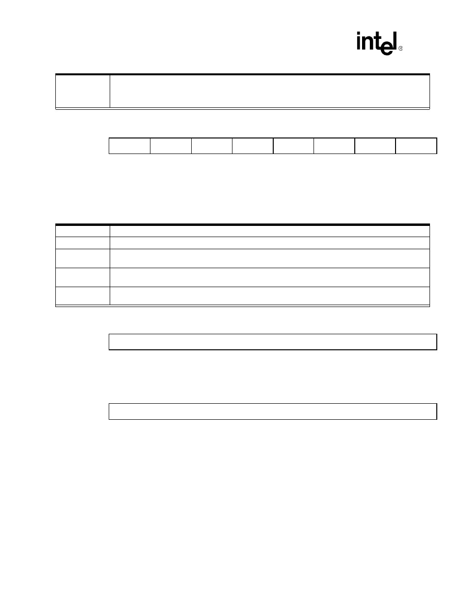
10.1.8 Interrupt Enable Register (IER)
This register is used to enable up to five types of UART interrupts: receiver line status, received data available, character time-out
indication (FIFO mode only), Transmitter Holding register empty, and modem status. Each enabled interrupt can individually
cause an interrupt to host on the
µP HINT output pin. To cause an interrupt to the host (HINT), both the interrupt enable bit and
OUT2 (MCR2) must be set
to ‘1’.
10.1.9 Transmitter Holding Register (THR)
The THR (Transmitter Holding register) is a write-only register used for sending data and AT commands to the modem.
10.1.10Receiver Buffer Register (RBR)
The RBR (Receiver Buffer register) is a read-only register used for receiving data and AT command responses from the modem.
Bit 0
Interrupt Pending–This bit indicates when a modem interrupt is pending. Whenever this bit is equal to
“0”, then one or more interrupts are pending. Whenever this bit is equal to “1”, then no interrupts are pend-
ing. When an interrupt has occurred, the host can determine the cause of the interrupt by looking at the
IIR interrupt ID bits 0 and 1 (and interrupt ID bit 2 for FIFO mode).
Bits 7:4
Not used–These bits are permanently set to “0”.
Bit 3
MSIE (Modem Status Interrupt Enabled)–when set to “1”, this bit enables the modem status interrupt.
Bit 2
RLSIE (Receiver Line Status Interrupt Enabled)–when set to “1”, this bit enables the receiver line sta-
tus interrupt.
Bit 1
THREIE (Transmitter Holding Register Empty Interrupt Enabled)–when set to “1”, this bit enables
the Transmitter Holding register empty interrupt.
Bit 0
RDAIE (Received Data Available Interrupt Enabled)–when set to “1”Programmer’s Guide, this bit
enables the received data available interrupt.
0
0
0
0
MSIE
RLSIE
THREIE
RDAIE
Register 1
(DLAB = 0)
THR
Register 0
(DLAB = 0)
RBR
Register 0
(DLAB = 0)