Interphase Tech iSPAN User Manual
Page 46
V.35 Interface
26
Interphase Corporation
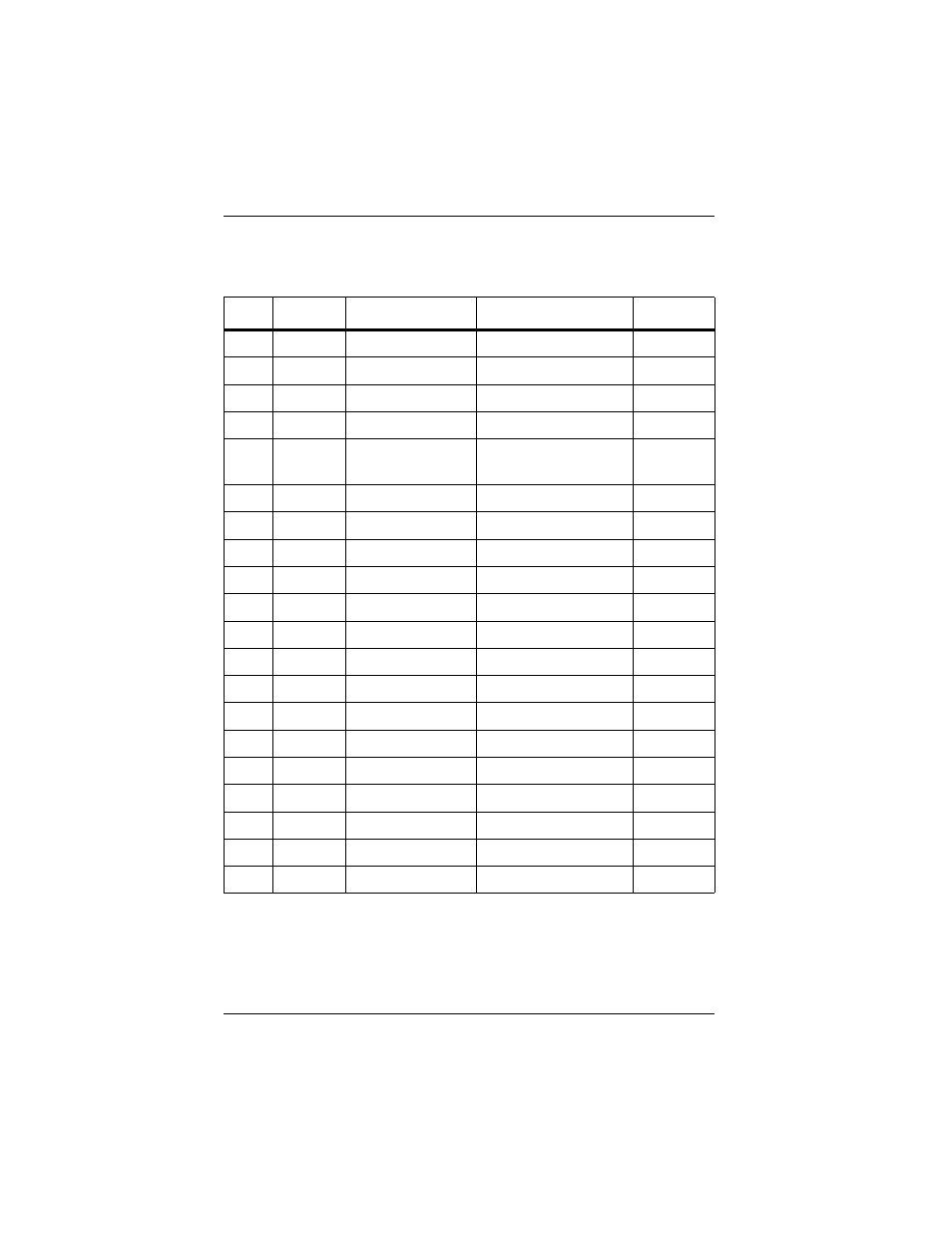
The following table and illustrations describe the V.35 signals
on the connector.
Pin # Tw. Pair
Name (CCITT #) Signal
Direction
2
I
TXD A (103 A)
Transmit Data
Out
14
I
TXD B (103 B)
Transmit Data
Out
3
II
RXD A (104 A)
Receive Data
In
16
II
RXD B (104 B)
Receive Data
In
24
III
TXCout A (113
A)
Transmit Clock (DTE)
Out
11
III
TXCout B (113 B) Transmit Clock (DTE)
Out
17
IV
RXC A (115 A)
Receive Clock
In
9
IV
RXC B (115 B)
Receive Clock
In
12
V
TXCin B (114 B)
Transmit Clock (DCE)
In
15
V
TXCin A (114 A)
Transmit Clock (DCE)
In
4
RTS(105)
Ready To Send
Out
5
CTS(106)
Clear To Send
In
6
DSR(107)
Data Set Ready
In
8
DCD(109)
Data Carrier Detect
In
20
DTR (108)
Data Terminal Ready
Out
22
RI(125)
Ring Indication
In
21
-ENV35
V.35 interface enable
In
25
-Test
Test
In
7
GND(102)
Ground
Common
1
Shield
Shield
Common