FUJITSU C145-C037-01EN User Manual
Page 52
5-4
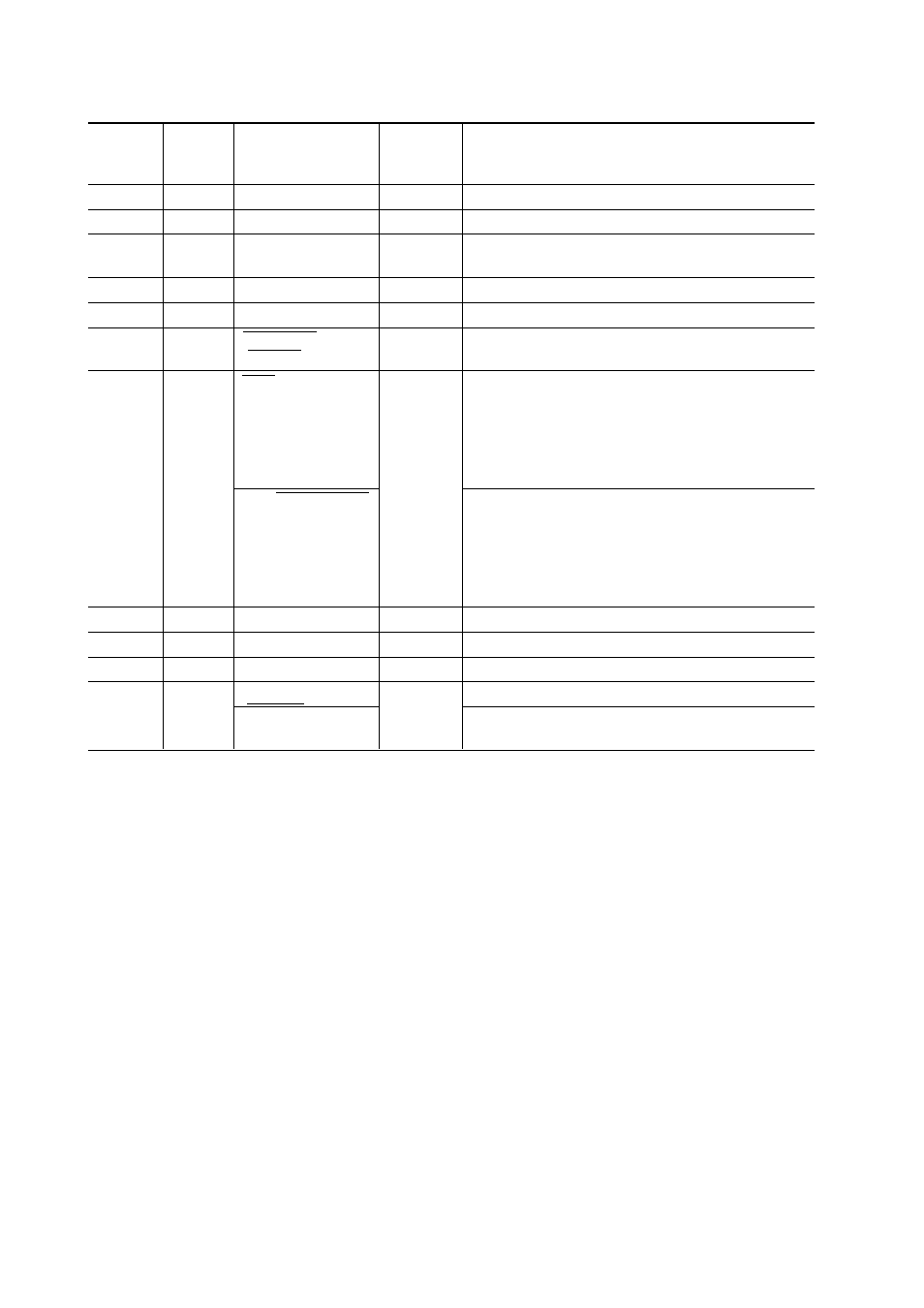
Connector
pin
number
15
16
17
18
19 to 30
31
32
33
34
35
36
Return
line pin
number
–
–
–
–
–
30
29
–
–
–
30
Direction
–
–
–
–
–
Input
Output
–
–
Output
Input
Description
Not used
Logic ground level (0 V)
Printer chassis ground line
FG and SG are connected.
Not used
Twisted-pair return lines
Reserved (*1)
This signal goes low under the following printer
conditions:
(1) Offline
(2) Paper out
(3) Cover open
(4) Other printer error
Reverse data transfer phase:
This signal is set low when the printer is ready to
send data to the host. During the data transfer, it is
used as data bit 0 (LSB), then data bit 4.
Reverse idle phase:
This signal is used to indicate that data is available.
Not used
Not used
Pulled up to +5 V through a 1.0 k
Ω
resistor
Reserved (*1)
This signal goes high to cause the printer to enter the
reverse data transfer phase (nibble mode).
Signal
Compati mode
Nibble mode
–
Signal Ground (SG)
Frame Ground (FG)
–
Signal Ground (SG)
Input Prime
(IN PRM)
Fault
Data Available
–
–
+5 V
(Select In)
1284 Active
Table 5.1 Parallel interface signals (continued)
*1 Assigned as a signal name, without any function.
Notes:
1.
Left-aligned signal names are in compati mode and right-aligned ones are in nibble mode.
2.
The direction (input and output) refers to the printer.
3.
Return line: Twisted-pair return line connected to the signal ground level