FUJITSU C145-C037-01EN User Manual
Page 50
5-2
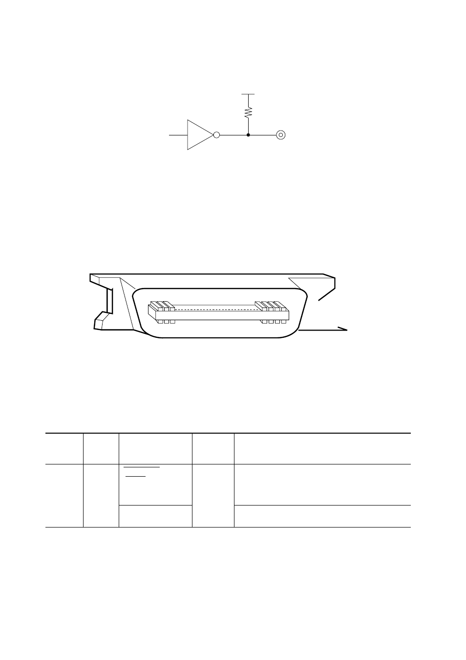
Figure 5.2 Parallel interface output circuit
5.2.2
Connector pin assignment
Connector (cable side): Shielded plug
Amphenol DDK57FE-30360 or equivalent
Figure 5.3 shows the parallel interface connector.
Output circuit: SN74LS06 or equivalent
Figure 5.2 shows the parallel interface output circuit.
Figure 5.3 Parallel interface connector (IEEE1284-B)
Signal definition:
Table 5.1 lists parallel interface signals and their functions.
Table 5.1 Parallel interface signals
+5 V
1
k
Ω
(Cable side)
(Male type)
36
18
1
19
Return
line pin
number
19
Signal
Compati mode
Nibble mode
Data Strobe
(DSTB)
Host Clock
Description
• Strobe pulse for reading data (Data 1 to Data 8).
The printer reads data when this signal is low.
• The pulse width must be 0.5
µ
s or more at the
printer’s receiving terminal.
This signal is set high when the host requests the
reverse data transfer phase (nibble mode).
Connector
pin
number
1
Direction
Input
- FTP-633GA1021 (6 pages)
- KA02038-Y820 (1 page)
- FTP-632MCL102 (7 pages)
- FTP-621MCL102 (6 pages)
- FTP-604 FTP-644MCL002 (7 pages)
- FTP-629MCL103-R (7 pages)
- FTP-641MCL351 (6 pages)
- FTP-030P (3 pages)
- FTP-627USL401 (9 pages)
- FTP-621CT001 (6 pages)
- FTP-629MCL054 (7 pages)
- FTP-634MCL001 (7 pages)
- FTP-624MCL002 (8 pages)
- Printer (4 pages)
- FTP-040HF Holder Series (2 pages)
- P3PC-1442-01EN (17 pages)
- FTP-631MCL201 (6 pages)
- FTP-628WSL120 (7 pages)
- ScandAll PRO P2WW-2410-01ENZ0 (45 pages)
- DL6400Pro (247 pages)
- FTP-632MCL003 (7 pages)
- FTP-633MCL400 (12 pages)
- FTP-631MCL302 (6 pages)
- 102 (8 pages)
- FTP-622MCL302 (6 pages)
- FTP-642MCL302 (7 pages)
- 16DV (39 pages)
- FTP-639MCL103/383-R (7 pages)
- FTP-637MCL401 (6 pages)
- DL9400 (250 pages)
- M304X (143 pages)
- FTP-631MCL352 (6 pages)
- FTP-631MCL101 (6 pages)
- FTP-639MCL353 (7 pages)
- FTP-641MCL302 (6 pages)
- FTP-622DCL001/011 (8 pages)
- FTP-628MCL401 (9 pages)
- FTP-621MCL201 (6 pages)
- FTP-641MCL101/102 (6 pages)
- FTP-632MCL301 (6 pages)
- DL3800 (262 pages)
- DL6400 (247 pages)
- FTP-627USL631 (10 pages)
- FTP-624MCL304 (7 pages)