Stac9200 block diagram – Endura RADISYS KP915GV User Manual
Page 40
KP915GV Product Manual
40
vol
mute
MUX
mute
vol
SD0
STAC9200 Block Diagram
AZALIA LINK LOGIC
Pin5
Pin8
Pin6
BIT_CLK
Pin11
Pin10
SYNC
SDI
Reset#
SPDIF
Receiver
Stream/
Channel
Select
Analog
PC Beep
Stream/
Channel
Select
Stream/
Channel
Select
Stream/
Channel
Select
Pin Complex
Pins 18/20
MIC In
Pin47
MUX
SPDIF IN
PCM to
SPDIF
OUT
Analog
Digital
SPDIF Pin48
Loop 1
HP
Out
HP
Out
+0dB
Line
Out
Line
Out
mute
-6dB
+22dB
vol
STEREO
ADC
DAC BYPASS MODE
Digital
PC Beep
MIC
Boost
Pin Complex
Pins 39/41
MONO_OUT
Pin 37
Pin Complex
Pins 21/22
Pin Complex
Pins 23/24
Pin Complex
Pins 35/36
Port A
Port D
Port C
Port B
Single Bit Loopback (Loop 3)
W
W
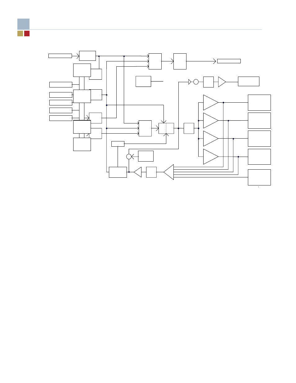
Figure 8.
SigmaTel STAC9200 High Definition Block Diagram
The audio Codec includes:
•
High performance Σ∆ technology
•
100dB DAC SNR
•
Intel HD Audio Interface
•
Two Channel DACs and ADCs with 24-bit resolution Sample rates up to 192kHz
•
Mixer-less design
•
Low-latency Karaoke Mode Supported
•
Integrated Headphone Amps
•
Stereo Microphone
•
Supports Stereo Mic
•
Microphone Boost 0, 10, 20, 30, 40dB
•
Direct CDROM Recording Mixerless Design
•
Universal Jacks (TM) Functionality for jack retasking
•
Adjustable VREF Out
•
Digital PC Beep to all outputs • +3.3V and +5V analog power supply options
•
32-pad QFN (5mm x 5mm) and 48-pin LQFP package options
Stream/
Channel
Select
Stream/
Channel
Select
Stream/
Channel
Select
Stream/
Channel
Select