17 post code technical description – Endura RADISYS KP915GV User Manual
Page 102
KP915GV Product Manual
102
Item
SMBIOS Data
Expected Result
23
Type 127: End-of-
Table
4.17
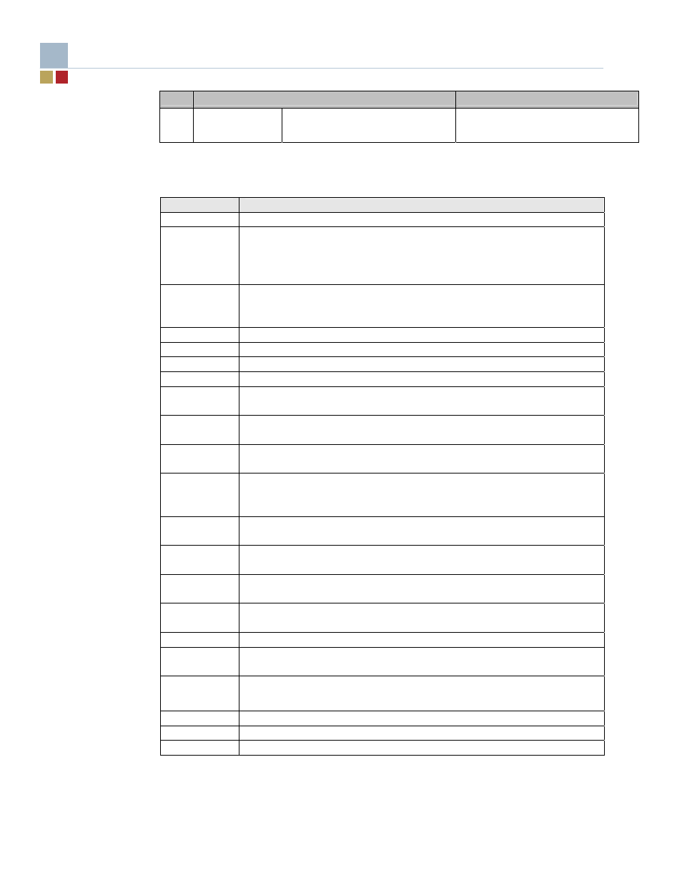
Post Code Technical Description
POST Code
Description
CFh
Test CMOS R/W functionality.
C0h
Early chipset initialization:
-Disable shadow RAM
-Disable L2 cache (socket 7 or below)
-Program basic chipset registers
C1h
Detect memory
-Auto-detection of DRAM size, type and ECC.
-Auto-detection of L2 cache (socket 7 or below)
C3h
Expand compressed BIOS code to DRAM
C5h
Call chipset hook to copy BIOS back to E000 & F000 shadow RAM.
01h
Expand the Xgroup codes locating in physical address 1000:0
03h
Initial Superio_Early_Init switch.
05h
1. Blank out screen
2. Clear CMOS error flag
07h
1. Clear 8042 interface
2. Initialize 8042 self-test
08h
Enable keyboard interface.
0Ah
Auto detect ports for keyboard & mouse followed by a port & interface swap
(optional).
0Eh
Test F000h segment shadow to see whether it is R/W-able or not. If test fails,
keep beeping the speaker.
10h
Auto detect flash type to load appropriate flash R/W codes into the run time
area in F000 for ESCD & DMI support.
12h
Use walking 1’s algorithm to check out interface in CMOS circuitry. Also set
real-time clock power status, and then check for override.
14h
Program chipset default values into chipset.
16h
Initial Early_Init_Onboard_Generator switch.
18h
Detect CPU information including brand, SMI type and CPU level.
1Bh
Initial interrupts vector table. If no special specified, all H/W interrupts are
directed to SPURIOUS_INT_HDLR & S/W interrupts to
SPURIOUS_soft_HDLR.
1Dh
Initial EARLY_PM_INIT switch.
1Fh
Load keyboard matrix (notebook platform)
21h
HPM initialization (notebook platform)