A.2 pci interrupt allocation – Endura RADISYS KP915GV User Manual
Page 107
KP915GV Product Manual
107
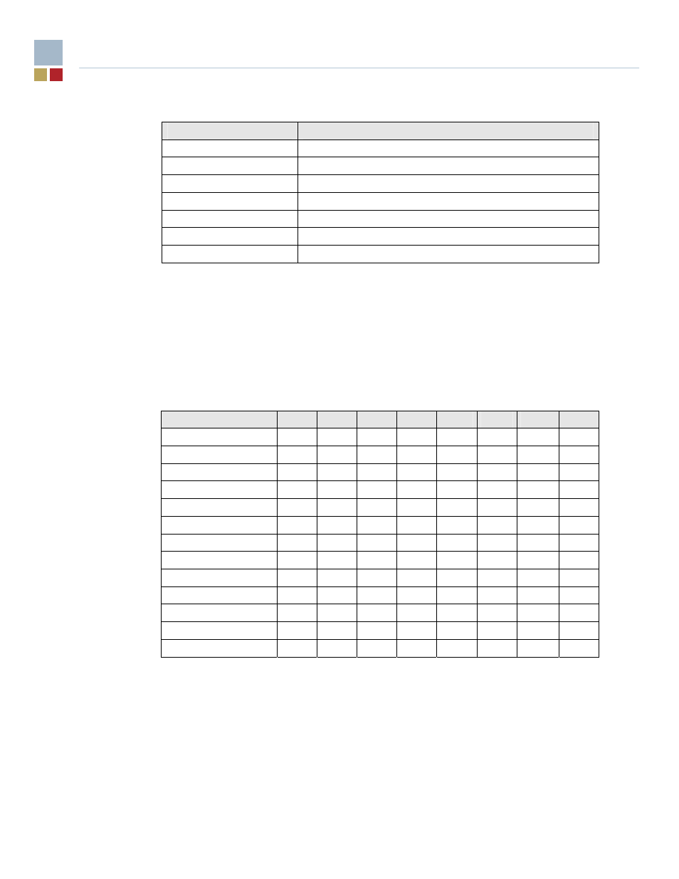
Table 8. I/O Map
Address (hex)*
Description
1300 – 133F
AC97 audio master
1800 – 182F
SIO GPIO and control logic
FFA0 – FFA7
Primary IDE bus master registers
FFA8 – FFAF
Secondary IDE bus master registers
Dynamically assigned
USB controller (four) (32 locations on 32-byte boundary)
Dynamically assigned
SMBus controller (16 locations on 16-byte boundary)
Dynamically assigned
LAN controllers (two) (4096 locations on a 4096-byte boundary)
* An ‘x’ prefix for the address indicates that only the low-order 10 address bits are decoded.
A.2
PCI Interrupt Allocation
In order to share PCI interrupts efficiently, the routing of the PCI interrupts INTA - INTD to the
motherboard PCI interrupts PIRQE – PIRQH are rotated for each slot. Thus the PCI card INTA
signals for the PCI slots are spread across these four motherboard inputs. Interrupt routing for the
riser slots is determined by the riser design.
Table 9. PCI Interrupt Allocation
Device
PIRQA PIRQB PIRQC PIRQD PIRQE PIRQF PIRQG
PIRQH
Slot
1
(AGP4X)
INTA
INTB
– – – – – –
Slot
2
(PCI
2.2)
– – – – INTA
INTB
INTC
INTD
Slot
3
(PCI
2.2)
– – – – INTD
INTA
INTB
INTC
Slot
4
(PCI
2.2)
– – – – INTC
INTD
INTA
INTB
VGA
controller
INTA
– – – – – – –
Ethernet
controller
1
INTA
– – – – – – –
Ethernet
controller
2
– INTA
– – – – – –
USB
UHCI
controller
1
INTA
– – – – – – –
USB
UHCI
controller
2
– – – INTB
– – – –
USB
UHCI
controller
3
– – INTC
– – – – –
USB
EHCI
controller
– – – – – – – INTD
SMBus
controller – INTB
– – – – – –
AC97
controller
– INTB
– – – – – –
Example.
From the previous table, the INTA interrupt from a card plugged into slot 2 would be
routed to the motherboard PIRQE.