A.3 pci device assignments, A.4 smbus resource allocation – Endura RADISYS KP915GV User Manual
Page 108
KP915GV Product Manual
108
A.3
PCI Device Assignments
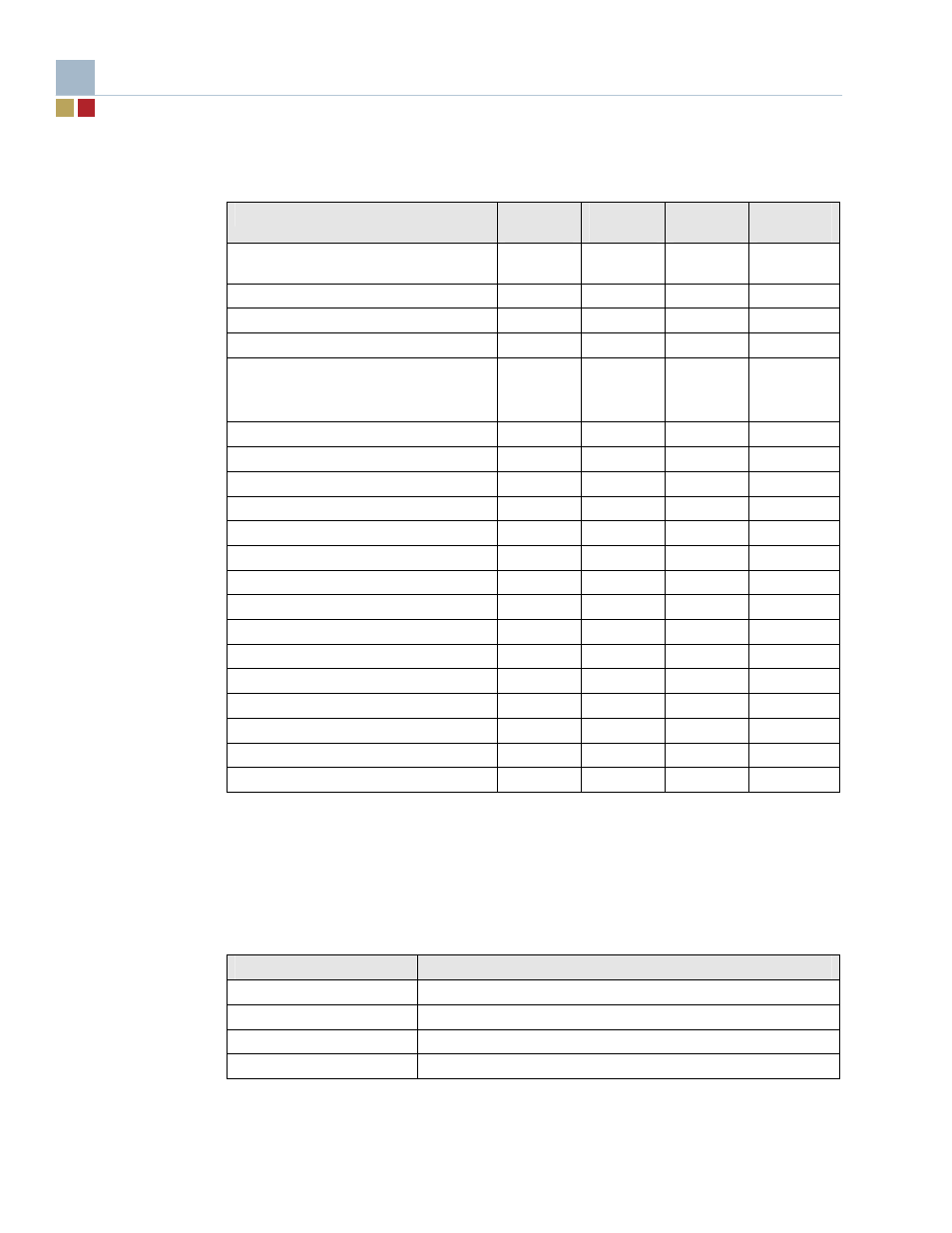
Table 10. PCI Device Assignments
Device
IDSEL
Bus
Number
Device
Number
Function
Number
Chipset host bridge and memory
controller
– 0 0 0
AGP
bridge
– 0 1 0
Graphics
controller
– 0 2 0
PCI
bridge
– 0 30 0
LPC bridge
(Includes DMA, timers, PIC, APIC, RTC,
power & system management, GPIO)
– 0 31 0
IDE
controller
– 0 31 1
SMBus
controller
– 0 31 3
AC97 audio controller
–
0
31
5
USB UHCI controller 1
–
0
29
0
USB UHCI controller 2
–
0
29
1
USB UHCI controller 3
–
0
29
2
USB EHCI controller
–
0
29
7
Slot 1 (AGP4X)
AD16
2
0
–
Slot 2 (PCI 2.2)
AD17
2
1
–
Slot 3 (PCI 2.2)
AD18
2
2
–
Slot 4 (PCI 2.2)
AD19
2
3
–
Slot 5 (PCI 2.2, via riser only)
AD20
2
4
–
Slot 6 (PCI 2.2, via riser only)
AD21
2
5
–
Ethernet controller 1
AD23
2
7
0
Ethernet controller 2
AD24
2
8
0
The PCI slots and the Ethernet controller are behind a virtual bridge to PCI bus 2 implemented by
the chipset ICH4. An AGP card, when present, resides on PCI bus 1.
A.4
SMBus Resource Allocation
Table 11. SMBus Resource Allocation
Address
Description
0101 110X
System management controller (LM85)
1010 000X
Memory module 1
1010 001X
Memory module 2
1101 001X
Clock synthesizer