6 915gv chipset feature, Processor/host interface (fsb), System memory controller – Endura RADISYS KP915GV User Manual
Page 26
KP915GV Product Manual
26
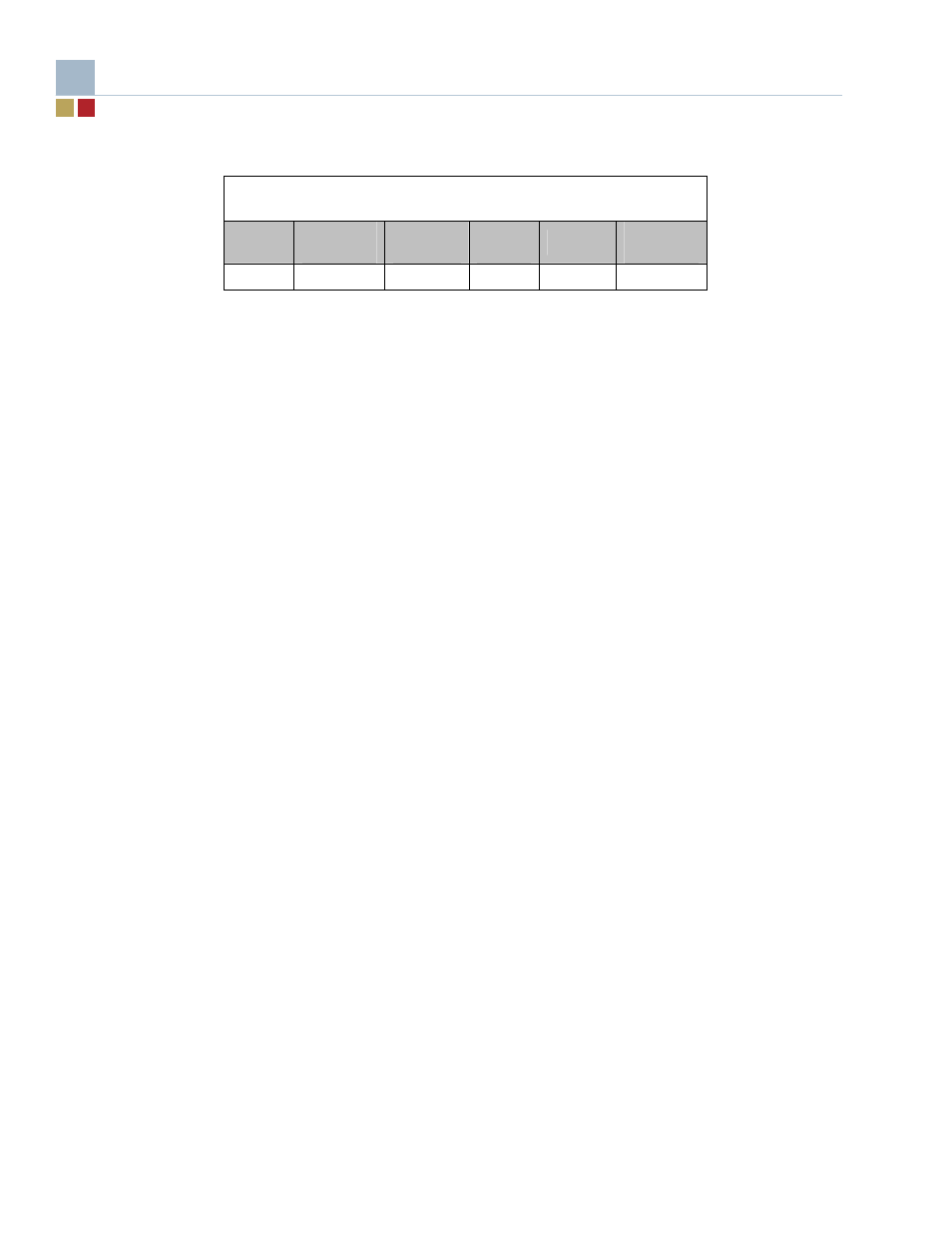
Table 1. KP915GV Motherboard
Chipset
Form
Factor
PCI-E x16
or ADD2
PCI-E
x1
PCI
PCI Riser
Extension
915GV ATX
1
2
3
N/A
•
See Figure 5 for slot configurations
•
ADD2 will be a green connector
2.6
915GV Chipset Feature
The 915GV is a Memory Controller Hub (MCH) designed for use with the Prescott processors in
desktop platforms. The role of a MCH is a system is to manage the flow of information between its
four interfaces: the CPU interface (FSB), the DDR/DDR2 System Memory interface (DRAM
controller), the External Graphics interface (PCI Express-G), and the I/O Controller through Direct
Media Interface (DMI). It’s 1210 Flip Chip Ball Grid Array (FCBGA) package.
Processor/Host interface (FSB)
•
Supports a single Pentium 4 processor with 1-MB L2 cache in the 90 nm process, in an
LGA775 package.
•
The primary enhancements over the Compatible Mode P6 bus protocol are:
1- Source synchronous double-pumped (2x) Address
2- Source synchronous quad-pumped (4x) Data
•
Supports Pentium 4 processor FSB interrupt delivery.
•
Supports Pentium 4 processor Front Side Bus (FSB) at the following Frequency Ranges:
533/800MT/s (133/200MHz)
•
Supports Hyper-Threading Technology (HT Technology)
•
Supports FSB Dynamic Bus Inversion (DBI)
•
Supports 36-bit host bus addressing, allowing the CPU to access the entire 4GB of the MCH’s
memory address space.
•
12-deep In-Order Queue to support up to twelve outstanding pipelined address requests on
the host bus.
•
1-deep Defer Queue.
•
Utilizes GTL+ bus driver with integrated GTL termination resistors.
•
Supports a Cache Line Size of 64 bytes.
•
At 133/200MHz bus clock the address signals run at 266/400MT/s, the data is quad pumped
and an entire 64B cache line can be transferred in two bus clocks. At 133/200MHz bus clock
the data signals run at 533/800MT/s for a maximum bandwidth of 4.3GB/s.
System Memory Controller
•
The MCH System Memory Controller directly supports dual channel of memory (each channel
consisting of 64 data lines)
1- The memory channels are asymmetric: “Stacked” channels are assigned address serially.
Channel B addresses are assigned after all Channel A addresses.
2- The memory channels are interleaved: Addresses are ping-ponged between the channels
after each cache line (64-B boundary).
•
Supports DDR2 memory DIMM frequencies of 400 and 533MHz. The speed used in all
channels is the speed of the slowest DIMM in the system.