Fpga design, Figure 18 - firmware block diagram – Sundance SMT950 User Manual
Page 47
Version 2.0
Page 47 of 52
SMT950 User Manual
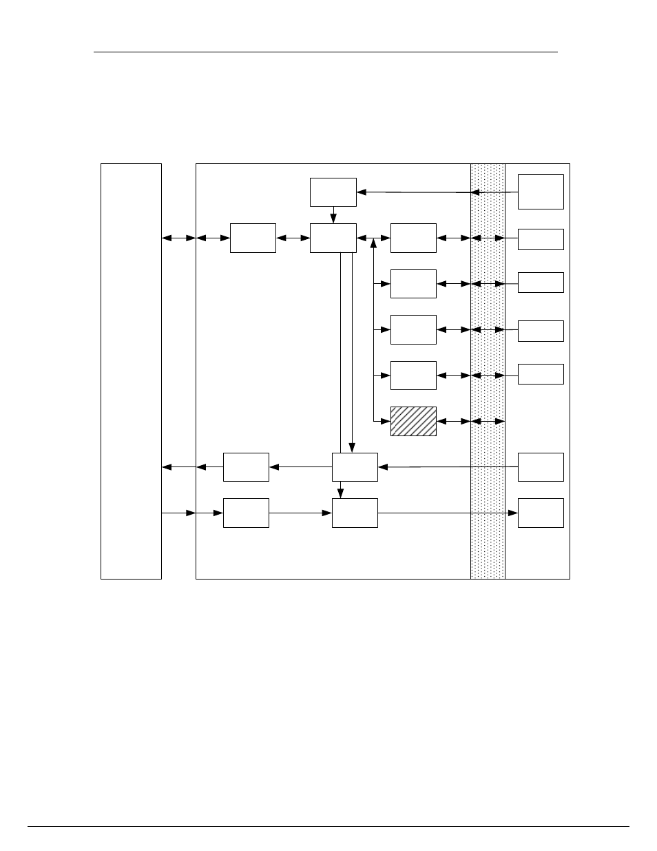
FPGA Design
The following block diagram shows how the default FPGA design is structured:
SLB
SMT368 Virtex-4 FPGA
Comport
Interface
Registers
ADCA Serial
Interface
ADCB Serial
Interface
DAC Serial
Interface
Clock Serial
Interface
Temperature
Serial
Interface
Route and
Format
Route and
Format
SHBB
Interface
SHBD
Interface
Trigger Block
SMT950
Other
Sundance
Module (DSP
Module
Usually)
DACs ChA
and ChB
data port
ADCs ChA
and ChB
data port
2x14 bits
2x16 bits
Ext. Trigger
ADC A&B
and DAC
A&B
ADCs ChA
SPI
ADCs ChB
SPI
DAC SPI
Clock SPI
Figure 18 - Firmware Block Diagram.
Serial Interfaces
All serial interfaces have been designed in accordance with manufacturers
datasheets and validated by probing and checking against timing provided.
- SMT107 (16 pages)
- SMT6035 v.2.2 (39 pages)
- SMT6012 v.4.6 (22 pages)
- FC100 (12 pages)
- FC108 v.1.1 (10 pages)
- SMT6065 v.4.0 (45 pages)
- FFT v.2.1 (19 pages)
- SMT111 (18 pages)
- SMT118LT (10 pages)
- SMT118 (20 pages)
- SMT123-SHB (13 pages)
- SMT128 (15 pages)
- SMT145 (18 pages)
- SMT148 (35 pages)
- SMT130 v.1.0 (46 pages)
- SMT148FX (48 pages)
- SMT310Q (55 pages)
- PARS (70 pages)
- SMT166-FMC (52 pages)
- SMT166 (44 pages)
- SMT300Q v.1.6 (61 pages)
- SMT310 v.1.6 (50 pages)
- SMT317 (24 pages)
- SMT326v2 (24 pages)
- SMT338 (19 pages)
- SMT349 (32 pages)
- SMT339 v.1.3 (27 pages)
- SMT338-VP (22 pages)
- SMT358 (25 pages)
- SMT351T (37 pages)
- SMT351 (25 pages)
- SMT350 (45 pages)
- SMT362 (30 pages)
- SMT365G (23 pages)
- SMT364 (37 pages)
- SMT373 (15 pages)
- SMT368 (24 pages)
- SMT370v3 (46 pages)
- SMT377 (22 pages)
- SMT381 2007 (31 pages)
- SMT381-VP (81 pages)
- SMT387 (42 pages)
- SMT391 (18 pages)
- SMT384 (47 pages)
- SMT390-VP (55 pages)