Sundance SMT950 User Manual
Page 31
Version 2.0
Page 31 of 52
SMT950 User Manual
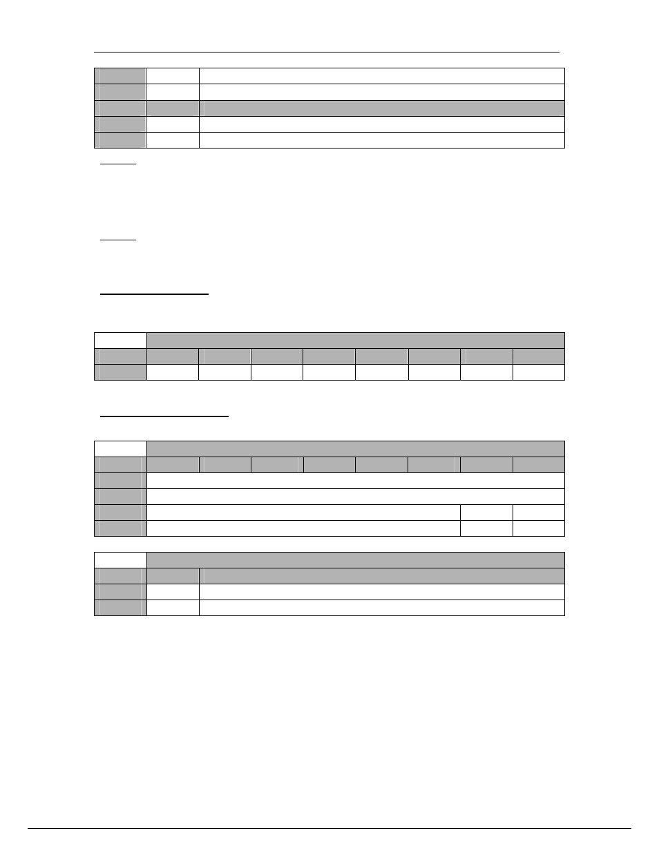
2
10
DAC PHSTR line is driven Low.
3
11
Normal Operation – DAC PHSTR is Tri-Stated.
Setting
Bit 5
Description
0
0
DDS Activated and SHB put on hold.
1
1
Resets DDS Core (SHB samples are routed to the DAC)
Note 1: What is mentioned as DAC PHSTR line is the physical net on the board that
connects together the FPGA to the PHSTR pin (DAC5687) as well as to J5 (+). In a
multiple board system, one board can be used as a master and its PHSTR pin can
be driven high or low and an other one as slave, in which case its DAC PHSTR pin
must be tri-stated.
Note 2: The Reset bits don’t get cleared automatically, so a device can remain reset
while not used to reduce the global power consumption.
Test Register – 0x1.
Any 8-bit value written in this register can be read-back to check that the Comport
used works properly.
Test Register – 0x1
Byte
Bit 7
Bit 6
Bit 5
Bit 4
Bit 3
Bit 2
Bit 1
Bit 0
0
ADCA Register 0 – 0x2.
For more details, refer to ADS5500 datasheet.
ADCA Register 0 – 0x2
Byte
Bit 7
Bit 6
Bit 5
Bit 4
Bit 3
Bit 2
Bit 1
Bit 0
1
Reserved
Default
‘0000000’
0
Reserved PLL
Reserved
Default
‘000000’ ‘0’
‘0’
ADCA Register 0 – 0x2
Setting
Bit 1
Description
0
0
PLL OFF – for sampling frequencies between 10 and 80 MHz
1
1
PLL ON – for sampling frequencies between 60 and 125 MHz