Dds register 0 – start phase increment lsb - 0x20 – Sundance SMT950 User Manual
Page 40
Version 2.0
Page 40 of 52
SMT950 User Manual
Updates, Read-back and Firmware Version Registers – 0x1D
The Update bit activates the corresponding Serial Interface to pass registers
previously written in the FPGA, into the corresponding device (ADCA, ADCB, DAC or
CLK devices).
The Read-back bit activates the corresponding Serial Interface to read-back register
values from the corresponding device and to pass them to the FPGA. This operation
must be followed by Read-back register operations.
Note that only the DAC allows proper read-back operation. Other devices read-back
commands would only perform a read-back of the FPGA register.
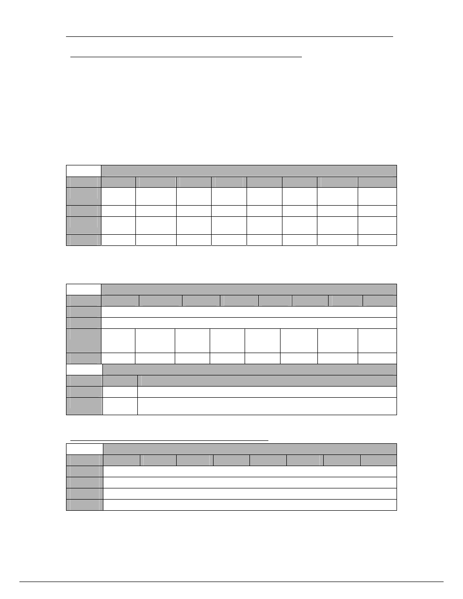
Update and Read-back commands – 0x1D
Byte
Bit 7
Bit 6
Bit 5
Bit 4
Bit 3
Bit 2
Bit 1
Bit 0
0
Reserved DDS
Step
Update
DDS Stop
Update
DDS Start
Update
CLK
Update
DAC
Update
ADCB
Update
ADCA
Update
Default
‘0’ ‘0’ ‘0’ ‘0’ ‘0’ ‘0’ ‘0’ ‘0’
1
DAC
Read-back
Default
‘0’ ‘0’ ‘0’ ‘0’ ‘0’ ‘0’ ‘0’ ‘0’
Reading-back this register returns the Firmware version as well as some Status
signals.
Firmware Version and Status – 0x1D
Byte
Bit 7
Bit 6
Bit 5
Bit 4
Bit 3
Bit 2
Bit 1
Bit 0
0
Firmware Version
Default
‘00000000’
1
DAC
Busy
read-back
CDCM7005
Status
VCXO
CDCM7005
Status Ref
CDCM7005
Status Lock
Default
‘0’ ‘0’ ‘0’ ‘0’ ‘0’ ‘0’ ‘0’ ‘0’
Firmware Version and Status – 0x1D
Setting
Bit 11
Description
0
‘0’ Normal
Mode
of
Operation
1
‘1’
DAC Busy – FPGA in the process of reading its internal registers. This bit can be used for polling
before read all registers from FPGA.
DDS Register 0 – Start Phase Increment LSB - 0x20
DDS Register 0 – 0x20
Byte
Bit 7
Bit 6
Bit 5
Bit 4
Bit 3
Bit 2
Bit 1
Bit 0
1
DDS Start Phase Increment[15…8]
Default
‘00000000’
0
DDS Start Phase Increment [7…0]
Default
‘00000000’