4 connectors, 1 description – Sundance SMT942 User Manual
Page 47
User Manual SMT942
Page 47 of 55
Last Edited: 23/08/2011 17:25:00
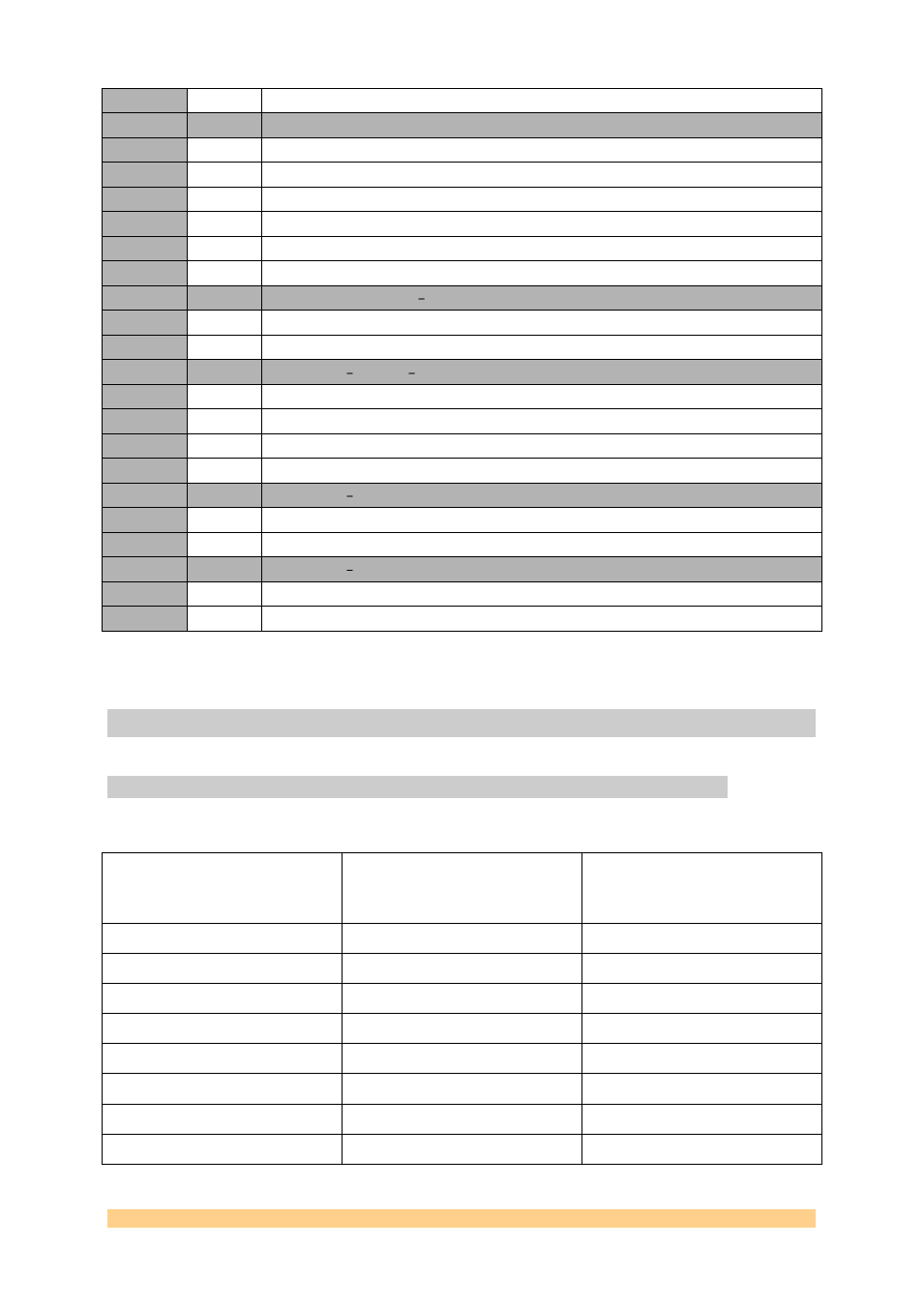
3
‘111’
n value=8.
Setting
Bit 7:3
Description - pll_m
0
‘00000’
m value=1.
1
‘00001’
m value=2.
2
‘00011’
m value=4.
3
‘00111’
m value=8.
4
‘01111’
m value=16.
5
‘11111’
m value=32.
Setting
Bit 11:8
Description - pll_range to adjust the vco current
0
‘0000’
Minimum bias current and lowest VCO frequency range.
1
’1111’
Maximum bias current and highest VCO frequency range.
Setting
Bit 13:12
Description pll_gain to adjust the vco gain (Kvco)
0
‘00’
1
‘01’
2
‘10’
3
‘11’
Setting
Bit 14
Description vco_div2
0
‘0’
PLL clock output is not divided.
1
’1’
PLL clock output is divided by 2.
Setting
Bit 15
Description pll_lpf_reset
0
‘0’
1
’1’
Holds the pll loop filter at 0 volts
4 Connectors
4.1 Description
The following table gathers all connectors on the board and describes their
function.
Connector
name
(silkscreen
and
schematics)
Description
Location on the board
J16
DACA Analog Output
Top / Left
J15
DACB Analog Output
Top / Left
J1016
DACC Analog Output
Top / Right
J1015
DACD Analog Output
Top / Right
J30
External Reference Input
Bottom / Right
J29
External Clock Input
Bottom / Left
J4
External Clock Output
Bottom / Left
J24
External Trigger
Bottom / Left