Dac chab register 1 0x41 – Sundance SMT942 User Manual
Page 39
User Manual SMT942
Page 39 of 55
Last Edited: 23/08/2011 17:25:00
Setting
Bit 13
Description clk1c_in_ena
0
0
Pin used as PLL_LOCK status output.
1
1
Pin used as a clock input.
Setting
Bit 14
Description clk1_in_ena
0
0
Pin used as CLK0 clock output.
1
1
Pin used as a clock input.
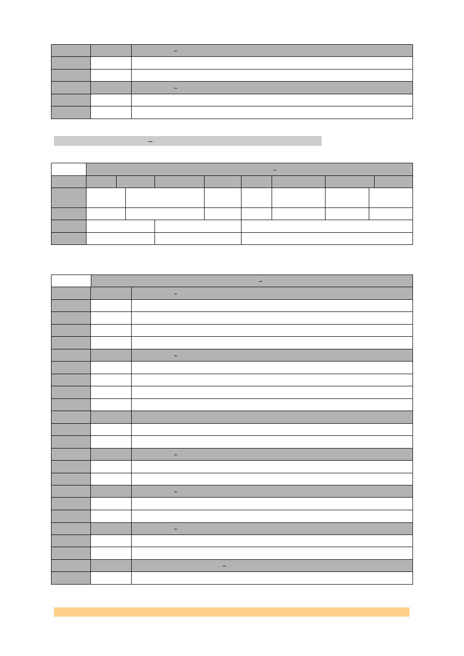
DAC Chab Register 1 0x41.
DAC Chab Register 1 0x41
Byte
Bit 7
Bit 6
Bit 5
Bit 4
Bit 3
Bit 2
Bit 1
Bit 0
1
Ser_dac_d
ata_ena
Output delay
b_equals
_a
A_equa
ls_b
reserved
revb
reva
Default
‘0’
‘00’
‘0’
‘0’
‘0’
‘0’
‘0’
0
Diffclk_dly
Clk0_dly
Reserved
Default
‘00’
‘00’
‘0000’
DAC Chab Register 1 0x41
Setting
Bit 5:4
Description clk0_dly
0
00
0ns delay.
1
01
1ns delay.
2
10
2ns delay.
3
11
3ns delay.
Setting
Bit 7:6
Description diffclk_dly
0
00
0ns delay.
1
01
1ns delay.
2
10
2ns delay.
3
11
3ns delay.
Setting
Bit 8
Description - reva
0
0
Normal mode.
1
1
PortA reversed.
Setting
Bit 9
Description revb
0
0
Normal mode.
1
1
PortB reversed.
Setting
Bit 11
Description a_equals_b
0
0
Normal mode.
1
1
DACA driven by DACB data.
Setting
Bit 12
Description b_equals_a
0
0
Normal mode.
1
1
DACB driven by DACA data
Setting
Bit 14:13
Description - output_delay delay the output to both DACs
0
0
0 clock cycles