Sundance SMT942 User Manual
Page 26
User Manual SMT942
Page 26 of 55
Last Edited: 23/08/2011 17:25:00
Default
‘0’
‘0’
‘0’
‘0’
‘1011’
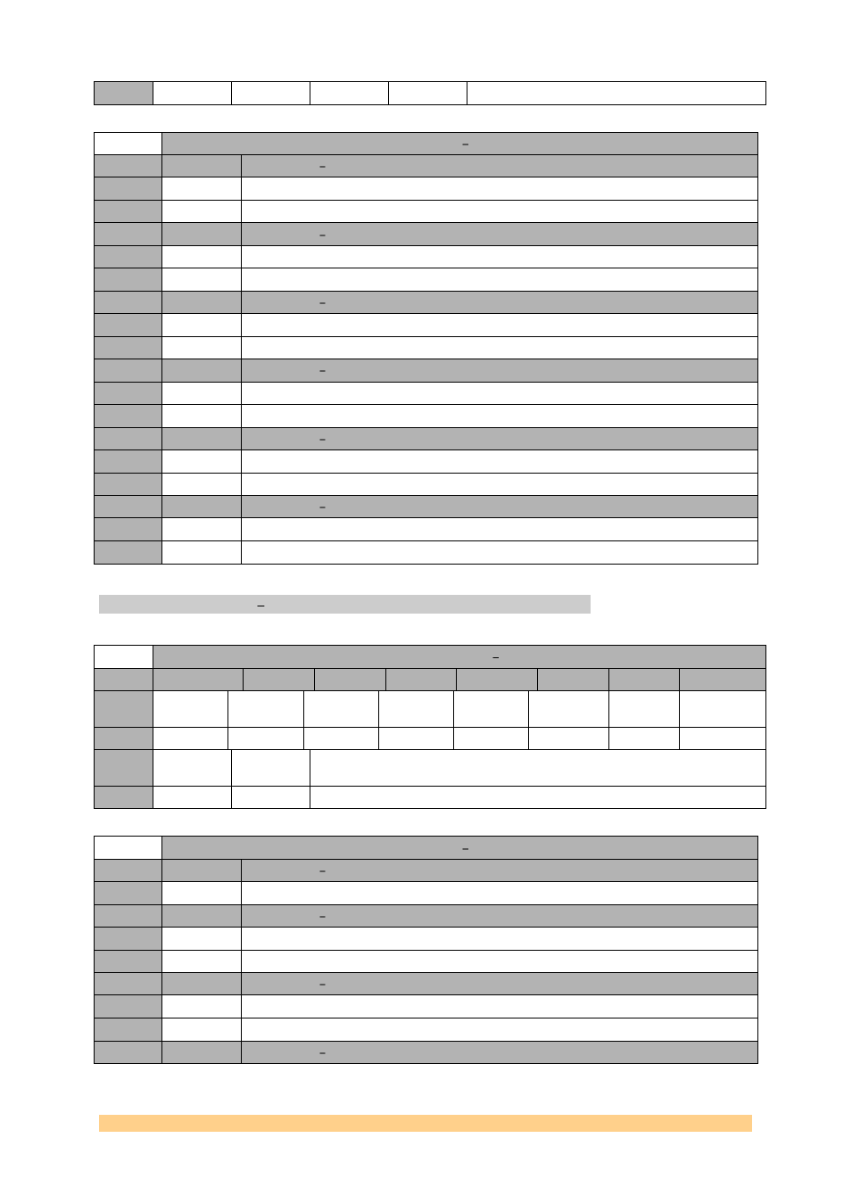
Reset Register 16 0x26
Setting
Bit 4
Description PRI_DIV2
0
‘0’
Primary reference divider disabled
1
‘1’
Primary reference divider enabled
Setting
Bit 5
Description SEC_DIV2
0
‘0’
Secondary reference divider disabled
1
‘1’
Secondary reference divider enabled
Setting
Bit 6
Description FB_DIS
0
‘0’
FB Divider is active
1
‘1’
FB Divider is disabled
Setting
Bit 7
Description FB_CML_SEL
0
‘0’
FB is CMOS type
1
‘1’
FB is CML type
Setting
Bit 8
Description FB_INCLK_INV
0
‘0’
Input clock for FB not inverted (normal/low speed mode)
1
‘1’
Input for FB inverted (high speed mode)
Setting
Bit 15:9
Description FB_COUNTER
0
‘0’
FB Path integer counter
1
CLOCK Register 17 0x27.
Clock Register 17 0x27
Byte
Bit 7
Bit 6
Bit 5
Bit 4
Bit 3
Bit 2
Bit 1
Bit 0
1
RESET_HO
LD
SEL_DELA
Y
RESHAPE
Reserved
OUT_MUX_S
EL
Default
‘0’
‘0’
‘0’
‘0’
‘0’
0
FB_MUX_S
EL
PD_PLL
FB_PHASE_ADJ
Default
‘0’
‘0’
‘000000’
Reset Register 17 0x27
Setting
Bit 5:0
Description FB_PHASE_ADJ
0
‘0’
Feedback phase adjustment
Setting
Bit 6
Description PD_PLL
0
‘0’
PLL in normal mode
1
‘1’
PLL powered down
Setting
Bit 7
Description FB_MUX_SEL
0
‘0’
VCXO selected for clock tree and FB
1
‘1’
External Clock selected for clock tree and FB
Setting
Bit 8
Description OUT_MUX_SEL