Clock register b 0x1b, Clock register c 0x1c – Sundance SMT942 User Manual
Page 21
User Manual SMT942
Page 21 of 55
Last Edited: 23/08/2011 17:25:00
1
Reserved
Reserved
Default
‘000000’
‘00’
0
Reserved
BIAS_DIV45
Reserved
Default
‘00’
‘00’
‘0101’
Reset Register A 0x1A
Setting
Bit 5:4
Description BIAS_DIV01 Current reduction output dividers 0 and 1
0
‘00’
No current output reduction
1
‘01’
20% output current reduction
2
‘10’
30% output current reduction
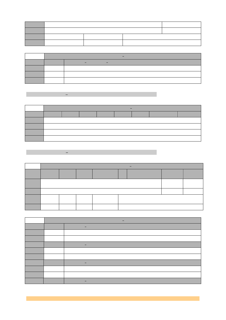
CLOCK Register B 0x1B.
Clock Register B 0x1B
Byte
Bit 7
Bit 6
Bit 5
Bit 4
Bit 3
Bit 2
Bit 1
Bit 0
1
Reserved
Default
‘01101000’
0
Reserved
Default
‘00000000’
CLOCK Register C 0x1C.
Clock Register C 0x1C
Byte
Bit 7
Bit 6
Bit 5
Bit 4
Bit
3
Bit 2
Bit 1
Bit 0
1
Reserved
DET_STAR
T_BYPASS
FB_START
_BYPASS
Default
‘000000’
‘0’
‘0’
0
DIV2_DIS
DIV_SEL
Reserve
d
FB_FD_DESEL
Reserved
Default
‘0’
‘0’
‘0’
‘0’
‘0110’
Reset Register C 0x1C
Setting
Bit 4
Description FB_FD_DESEL
0
‘0’
Feedback frequency detector is connected to the lock detector
1
‘1’
Feedback frequency detector is disconnected from the lock detector
Setting
Bit 6
Description DIV_SEL
0
‘0’
FB Clock divided by 1
1
‘1’
FB Clock divided by 2
Setting
Bit 7
Description DIV2_DIS
0
‘0’
Normal mode of operation
1
‘1’
FB Div2 in reset
Setting
Bit 8
Description FB_START_BYPASS