1 control packet structure, 3 interface description, 4 fpga design – Sundance SMT942 User Manual
Page 12: 1 mechanical interface 3.3.2 electrical interface
User Manual SMT942
Page 12 of 55
Last Edited: 23/08/2011 17:25:00
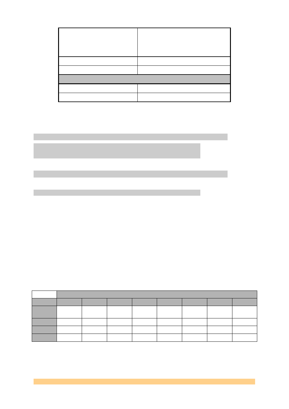
Input Voltage Level
1.5-3.3 Volts peak-to-peak.
Format
DC-coupled and Single-ended (Termination
implemented at the connector). Differential
on option (3.3 V PECL).
Impedance
50-Ohm.
Frequency range
62.5 MHz maximum
Delay
External Ref. Input to Ext Ref. Out
External Clk Input to Ext Clk Out
9ns (between J29 and J4)
Figure 2 - Clock Architecture Main Characteristics.
3.3 Interface Description
3.3.1 Mechanical Interface
3.3.2 Electrical Interface
3.4 FPGA Design
3.4.1 Control Register Settings
The Control Registers control the complete functionality of the SMT942. They are
setup via the Comport3 (standard firmware provided). The settings of the DACs,
triggers, clocks and the configuration of the interfaces and the internal FPGA data
path settings can be configured via the Control Registers.
3.4.1.1 Control Packet Structure
The data passed on to the SMT942 over the Comport must conform to a certain
packet structure. Only valid packets will be accepted and only after acceptance of a
packet will the appropriate settings be implemented. Each packet will start with a
command (4 bits – 0x1 for a write operation – 0x2 for a read operation) information,
followed by a register address (12 bits – see table Memory Map), followed by a 16-bit
data. This structure is illustrated in the following figure:
Byte Content
Byte
Bit 7
Bit 6
Bit 5
Bit 4
Bit 3
Bit 2
Bit 1
Bit 0
3
Command
3
Command
2
Command
1
Command
0
Address
11
Address
10
Address 9
Address 8
2
Address 7
Address 6
Address 5
Address 4
Address 3
Address 2
Address 1
Address 0
1
Data 15
Data 14
Data 13
Data 12
Data 11
Data 10
Data 9
Data 8
0
Data 7
Data 6
Data 5
Data 4
Data 3
Data 2
Data 1
Data 0
Figure 3
– Setup Packet Structure.