Clock register 0 0x10, Clock register 1 0x11 – Sundance SMT942 User Manual
Page 15
User Manual SMT942
Page 15 of 55
Last Edited: 23/08/2011 17:25:00
Setting
Bit 7
Description chcd trigger selection
0
0
Trigger from control register selected.
1
1
Trigger from external source selected.
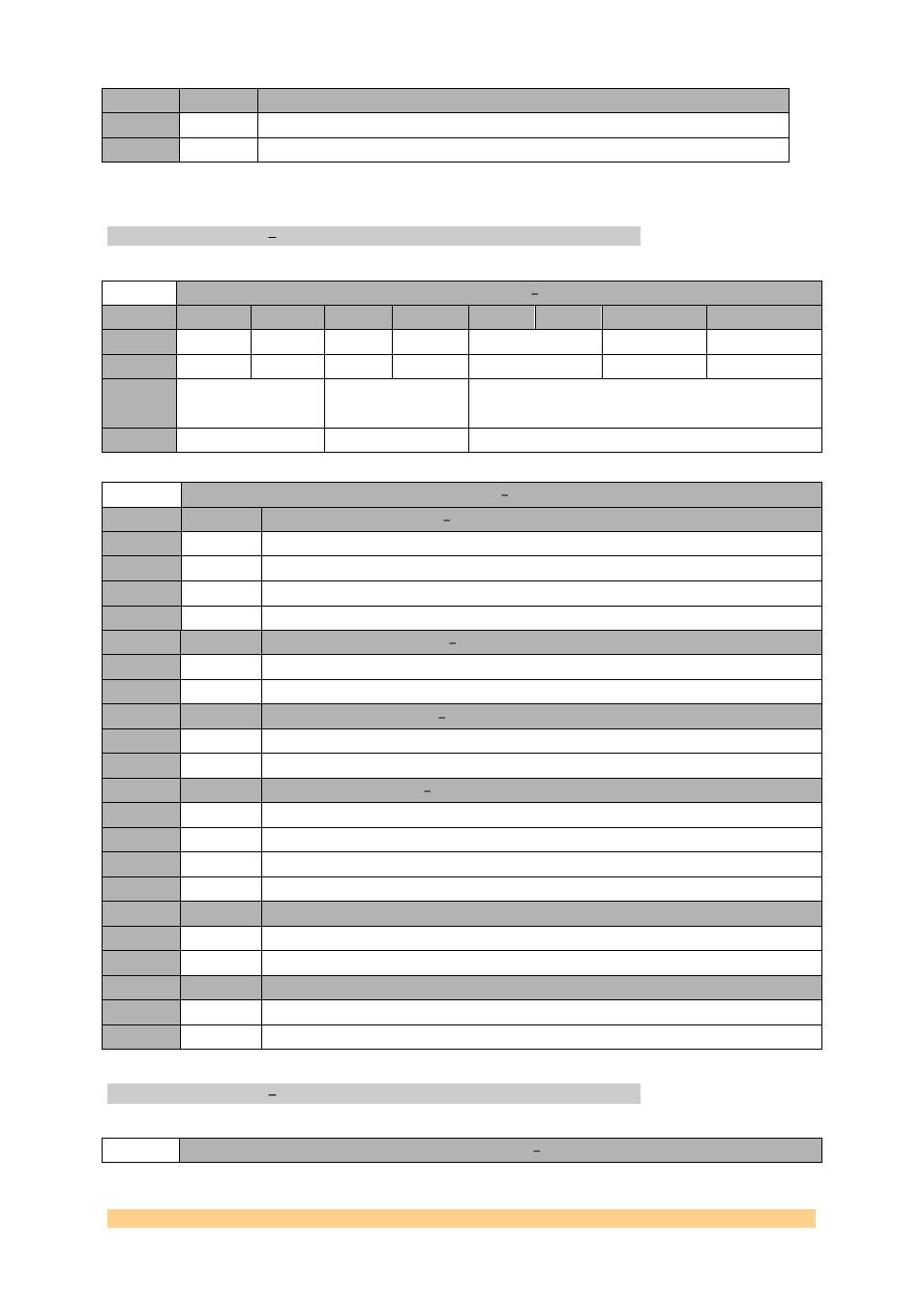
CLOCK Register 0 0x10.
Clock Register 0 0x10
Byte
Bit 7
Bit 6
Bit 5
Bit 4
Bit 3
Bit 2
Bit 1
Bit 0
1
Reserved
Reserved
CP_DIR
CP_MODE
DELAY_PFD
REFSELCNTRL
VCXO_AUX_SEL
Default
‘0’
‘0’
‘0’
‘0’
‘00’
‘0’
‘0’
0
SECSEL_PRISEL
Reserved
Reserved
Default
‘00’
‘00’
‘0000’
Clock Register 0 0x10
Setting
Bit 7:6
Description SECSEL_PRISEL Reference Input Selection
0
00
Nothing Selected
1
01
On-board Reference selected
2
10
External Reference selected
3
11
Auto Selection (Not recommended)
Setting
Bit 8
Description VCXO_AUX_SEL VCXO/AUX Selection
0
0
On-board or External Reference. Selected (SECSEL_PRI_SEL)
1
1
On-board VCXO or External Clock selected.
Setting
Bit 9
Description REFSELCNTRL Reference selection mode
0
0
Reference selection made externally.
1
1
Reference selection made internally (using SECSEL_PRISEL.).
Setting
Bit 11:10
Description DELAY_PFD PFD pulse width
0
00
1
01
2
10
3
11
Setting
Bit 12
Description CP_MODE
0
0
3V.
1
1
5V
Setting
Bit 13
Description CP_DIR
0
0
Positive CP current output
1
1
Negative CP current output
CLOCK Register 1 0x11.
Clock Register 1 0x11