Sundance SMT350 User Manual
Page 36
Version 1.9
Page 36 of 45
SMT350 User Manual
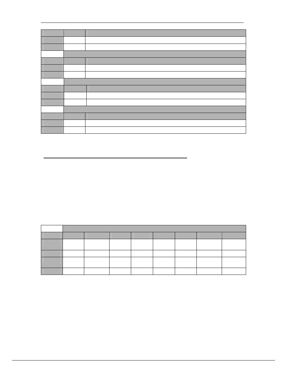
Setting
Bit 3
Description
0
0
Internal ADC Trigger set to ‘0’.
1
1
Internal ADC Trigger set to ‘1’.
Miscellaneous Register – 0x1C
Setting
Bit 2
Description
0
0 Binary
Format.
1
1 2’s
Complement.
Miscellaneous Register – 0x1C
Setting
Bit 1
Description
0
0 VCXO
selection.
1
1 External
Source
Selected.
Miscellaneous Register – 0x1C
Setting
Bit 0
Description
0
0
On-Board 10-MHz Reference Clock selected.
1
1 External
Reference
Selected.
Updates, Read-back and Firmware Version Registers – 0x1D
The Update bit activates the corresponding Serial Interface to pass registers
previously written in the FPGA, into the corresponding device (ADCA, ADCB, DAC or
CLK devices).
The Read-back bit activates the corresponding Serial Interface to read-back register
values from the corresponding device and to pass them to the FPGA. This operation
must be followed by Read-back register operations.
Note that only the DAC allows proper read-back operation. Other devices read-back
commands would only perform a read-back of the FPGA register.
Update and Read-back commands – 0x1D
Byte
Bit 7
Bit 6
Bit 5
Bit 4
Bit 3
Bit 2
Bit 1
Bit 0
0
Reserved DDS
Step
Update
DDS Stop
Update
DDS Start
Update
CLK
Update
DAC
Update
ADCB
Update
ADCA
Update
Default
‘0’ ‘0’ ‘0’ ‘0’ ‘0’ ‘0’ ‘0’ ‘0’
1
DAC
Read-back
Default
‘0’ ‘0’ ‘0’ ‘0’ ‘0’ ‘0’ ‘0’ ‘0’
Reading-back this register returns the Firmware version as well as some Status
signals coming from the CDCM7005.