Functional description, Figure 2 - block diagram – Sundance SMT350 User Manual
Page 10
Version 1.9
Page 10 of 45
SMT350 User Manual
Functional Description
In this part, we will see the general block diagram and some comments on some the
SMT350
entities.
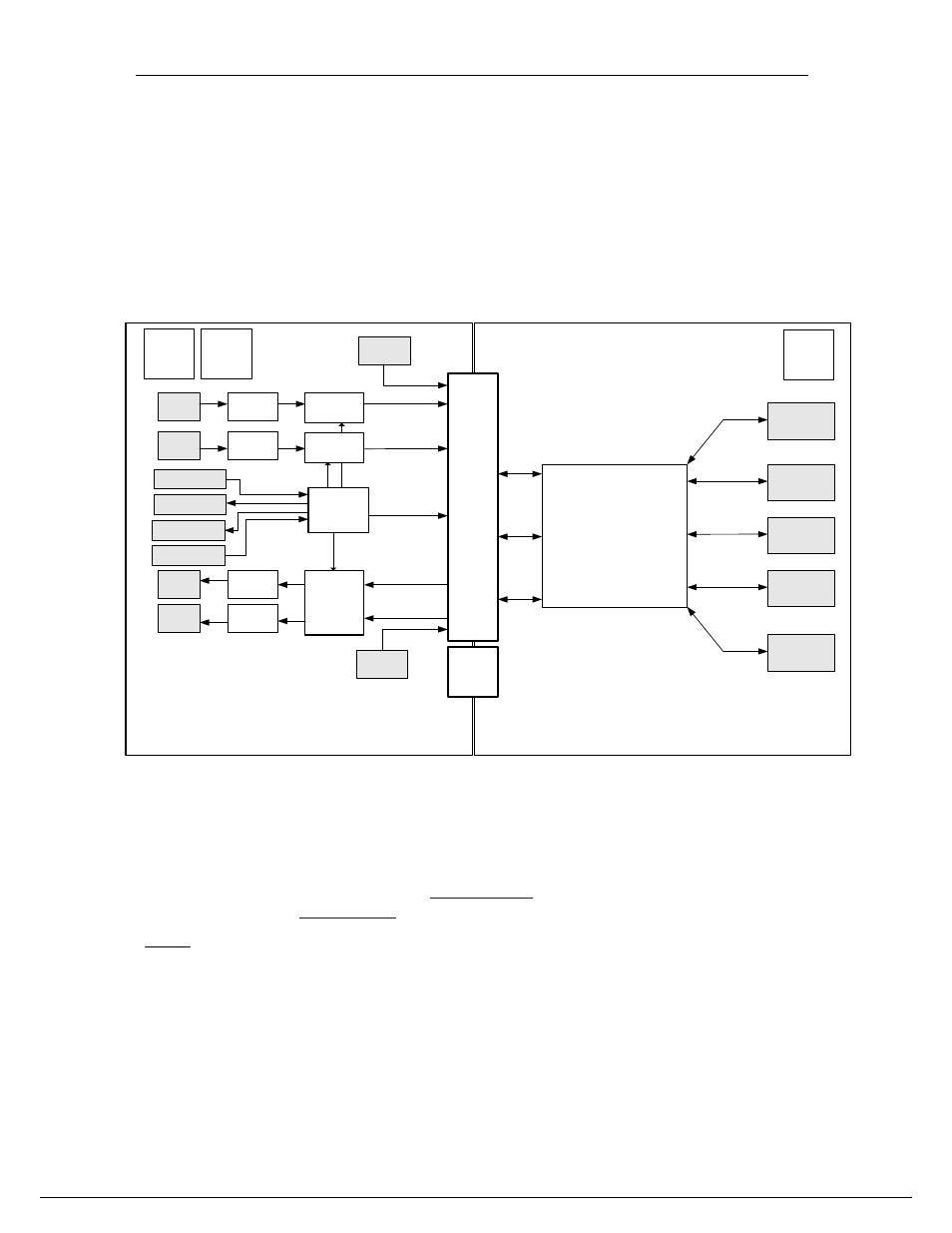
Block Diagram
The following diagram describes the architecture of the SMT350, coupled – as an
example – with an SMT368 to show how mezzanine and base modules are
connected together:
SMT368
SMT350
Virtex-4
XCV4SX35
FF668 Package
448 IOs
Channel A
Signal
Conditioning
Channel B
Signal
Conditioning
ADC Input
Ch A MMCX
50-Ohm
ADC Input
Ch B MMCX
50-Ohm
Daughter Card
interface
connector
SLB
Spare SHB connector
(SHBA)
Spare SHB connector
(SHBC)
SHBB
ADC Channel A and
Channel B
SHBD
DAC Channel A and
Channel B
Top and Bottom TIM
Connectors
ChA Data(14),
Clock and Control
ChA&ChB Data, Clock
and Control (60)
ChA&ChB Data, Clock
and Control (60)
2xComports and
Control (24)
ADS5500
ADC ChA
14-bit 125MSPS
ADS5500
ADC ChB
14-bit 125MSPS
Channel A
Signal
Conditioning
Channel B
Signal
Conditioning
DAC Output
Ch A MMCX
50-Ohm
DAC Output
Ch B MMCX
50-Ohm
DAC5686
Dual Channel DAC
16-bit 500MSPS
Interpolation
Power
Daughter Card
connector
SLB
ChB Data (16)
and Control
ChA Data (16)
and Control
Bank A
Bank B
Bank C
Power
Supplies: 1.8
and 3.3 Volts
Power
Supplies: 1.25,
1.5, 2.5 and 3.3
Volts
External ADC
Trigger
External ADC
Trigger
PECL Clock
Generation and
Distribution
based on
CDCM7005
and
SN65LVPC23
ADCs and DAC External
Clock In - MMCX
External Reference
Clock Out - MMCX
External Reference
Clock In - MMCX
DAC Clock
ChB Data(14),
Clock and Control
Temperature
Sensors
ADCs and DAC External
Clock Out - MMCX
Figure 2 - Block Diagram.
Module Description
The module is built around two
TI ADS5500
14-bit sampling analog-to-digital
converters and one
TI DAC5686
dual 16-bit digital-to-analog converter.
ADCs: Analog data enters the module via two MMCX connectors, one for each
channel. Both signals are then conditioned (AC coupling; DC optional) before being
digitized. Both ADCs gets their own sampling clock, which can be either on-board
generated or from an external reference or an external clock, common to ADCs and
DAC (MMCX connector). Digital samples travel to the FPGA on the base module via