Chapter 5 - programmer's guide, A programmer’s view of tempbook operations, Programmer's guide – Measurement Computing TempBook rev.3.0 User Manual
Page 29
Programmer's Guide
5
TempBook User’s Manual
Programmer's Guide 5-1
This and the following chapters are written for users who wish to write their own programs to control and
acquire data from the TempBook/66. This introductory chapter covers basic TempBook operation from a
programmer’s perspective and the options available for API drivers and languages. Further detail is
included through examples in the individual language support chapters, the command reference section, as
well as the chapters on thermocouple linearization and software calibration & zero compensation.
A Programmer’s View of TempBook Operations
The TempBook provides flexible, high-speed, multi-channel data acquisition capabilities through the use of
sophisticated analog and digital electronic circuitry. This circuitry allows up to 16 analog input channels to
be read at an aggregate 100 kHz sampling frequency. Each of these channels can be read as a unipolar (0 to
+V) or bipolar (±V) signal in one of 8 input voltage ranges. These ranges are determined by dividing the
standard 0 to 10V unipolar or ±5V bipolar input range by the available gains of ×1, 2, 5, 10, 20, 50, 100, or
200. Additionally, each input can be read as a single-ended or differential signal (selecting differential
limits the number of available channels to 8).
The conversion of these input signals to a digital code is accomplished by a high-performance 12-bit
analog-to-digital converter (ADC). (The resultant digital code can then be converted into a voltage via a
DAC). The output of the ADC is an unsigned value which is left-
justified within a 16-bit data word. In unipolar and bipolar modes,
the output code is related to the input voltage as shown in the table
(12-bit data format and standard input range shown).
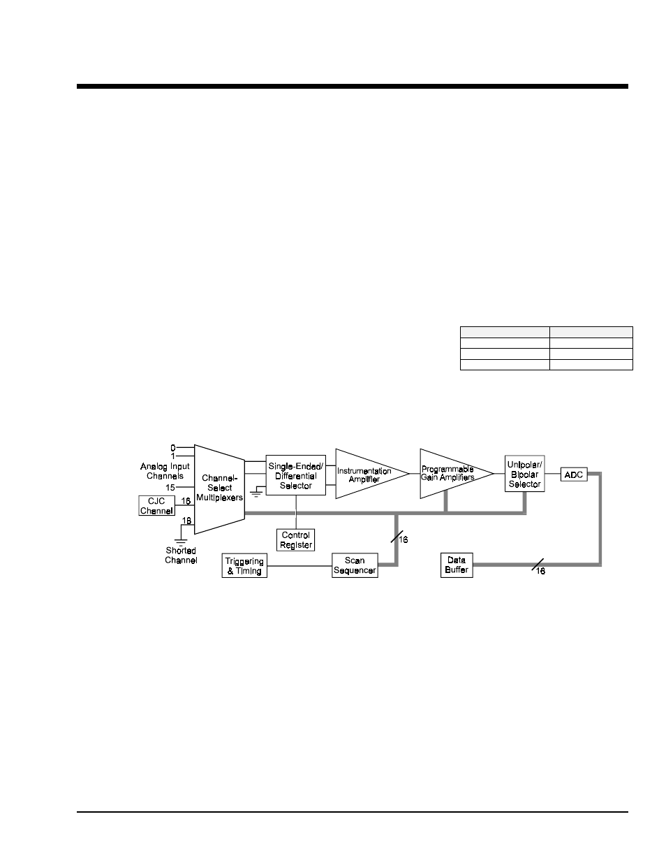
The analog section of the TempBook consists of the following: channel select multiplexers, a single-ended /
differential selector, an instrumentation amplifier, programmable gain amplifiers, a unipolar / bipolar
selector, and the 12-bit ADC.
Block Diagram
The analog electronics are controlled by a scan-sequencer and control registers. The scan sequencer is
implemented with a 16-bit × 512-location FIFO RAM. Each entry in the scan sequencer contains channel,
gain, and polarity information. The single-ended/differential selection is controlled by a static control
register entry. Once triggered, the scan sequencer is stepped through at a constant rate of 100 kHz until all
sequencer entries have been read. At each step, an ADC conversion is performed and the resultant output is
stored in a data buffer implemented with another 16-bit × 512-location FIFO RAM.
A scan is initiated by a trigger from a software command, a TTL input, or an internal pacer clock. In
addition to the source, a mode (one-shot or continuous-trigger) can be selected.
•
In one-shot mode, the scan sequencer is stepped through once (scanned) each time a trigger is
received.
•
In continuous mode, the scan sequencer waits for the selected trigger for the initial scan but
subsequent scans are initiated by the pacer clock.
Note: the selection of one-shot or continuous mode has no effect if the pacer clock is selected as the trigger
source.
Bipolar
Unipolar
0x000 = -5V
0x000 = 0V
0x800 = 0V
0x800 = 5V
0xFFF = 4.9976V
0xFFF = 9.9976V