Analog input calibration, External clock input – Measurement Computing LGR-5320 Series User Manual
Page 30
LGR-5320 Series User's Guide
Specifications
30
Note 3:
When connecting differential inputs to floating voltage sources in the ±10 V, ±5 V, ±1 V ranges, the
user must provide a DC return path from the low channel (CHxL) connector of each differential input
to ground. To do this, simply connect a resistor from the CHxL connector of the differential inputs to
AGND. A value of approximately 100
kΩ can be used for most applications.
The ±30 V input range on the LGR-5327/5329 incorporates an input resistor attenuator network, which
eliminates the need for external bias return compensation resistors.
Note 4:
The LGR-5325 AGND and GND pins are tied together internally. These grounds are electrically
isolated from the EGND (earth ground) pin.
The LGR-5327 AGND, GND and ENC- pins are tied together internally. These grounds are
electrically isolated from the EGND (earth ground) pin.
The LGR-5329 AGND, GND and ENC– pins are tied together internally. These grounds are
electrically isolated from the EGND (earth ground) and the IGND (isolated ground) pins.
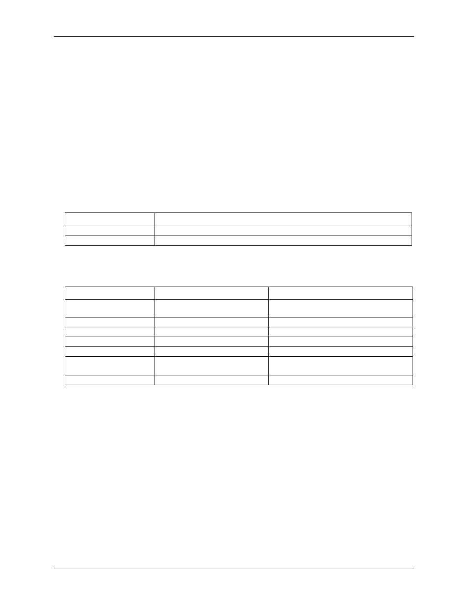
Analog input calibration
Table 2. Analog input calibration specifications
Parameter
Specifications
Calibration method
Factory calibration
Calibration interval
1 year
External clock input
Table 3. External clock I/O specifications
Parameter
Condition
Specification
External clock I/O
PACER (pin 75), software-selectable as input or
output
Input high voltage
2.2 V max
Input low voltage
0.6 V min
Output high voltage
IOH = –8 mA
3.8 V min
Output low voltage
IOL = 8 mA
0.4 V max
Pacer rate
LGR-5325: 100 kHz max
LGR-5327/5329:200 kHz max
Minimum pulse width
2.5 us min