Specifications, Analog input, Chapter 4 – Measurement Computing LGR-5320 Series User Manual
Page 29
29
Chapter 4
Specifications
All specifications are subject to change without notice.
Typical for 25 °C unless otherwise specified.
Specifications in italic text are guaranteed by design.
Analog input
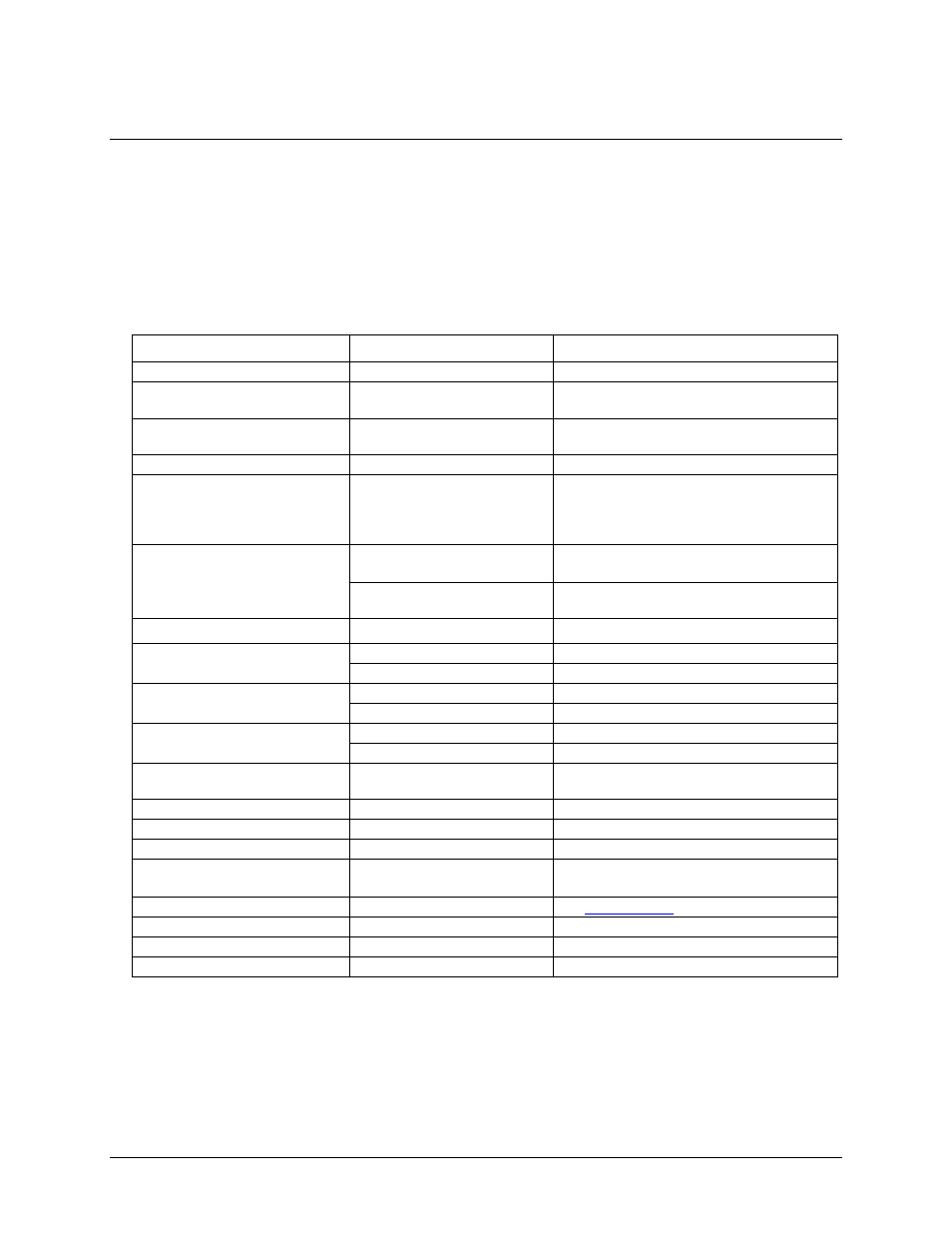
Table 1. Analog input specifications
Parameter
Condition
Specification
A/D converter
16-bit successive approximation type
Input ranges
Software selectable per channel
LGR-5327/5329: ±30 V, ±10 V, ±5 V, ±1 V
LGR-5325: ±10 V, ±5 V, ±1 V
Number of channels
8 differential (DIFF)/16 single-ended (SE),
software-selectable
Input configuration
Multiplexed
Absolute maximum input voltage
CHx_x to AGND
LGR-5327/5329: ±38 V max(power on and
power off)
LGR-5325: ±25 V max(power on and power
off)
Input impedance
±30 V range
(LGR-5327/5329 only)
1
MΩ (power on),
1
GΩ (power off)
±10 V, ±5 V, ±1 V range
10
GΩ (power on)
1
GΩ (power off)
Input leakage current
±100 pA
Input capacitance
±30 V range (LGR-5327/5329)
90 pf (Note 2)
±10 V, ±5 V, ±1 V range
55 pf
Maximum working voltage
(signal+ common mode)
±30 V range
±30.05 V
±10 V, ±5 V, ±1 V range
±10.2 V
Common mode rejection ratio
fin = 60 Hz, ±30 V range
65 dB min
fin = 60 Hz, all other ranges
75 dB min
Crosstalk
DC to 25 kHz, adjacent DIFF
mode channels
–80 dB
ADC resolution
16 bits
Input bandwidth (–3 dB)
All input ranges
450 kHz min
Input coupling
DC
Maximum sample rate
LGR-5327/5329: 200 kS/s
LGR-5325: 100 kS/s
A/D pacing sources
See
Warm up time
30 minutes, min
Absolute accuracy
All ranges
0.07% FSR
Noise
DIFF mode
2 LSB rms
Note 1:
Unused analog input channels can either be left floating or tied to an AGND pin.
Note 2:
When using the ±30 V input range, keep source impedance and source capacitance as small as possible
to minimize settling time, gain, and bandwidth errors.