The clock control, The clock control –21 – Altera Transceiver Signal Integrity User Manual
Page 45
Chapter 6: Board Test System
6–21
The Clock Control
February 2013
Altera Corporation
Transceiver Signal Integrity Development Kit,
Stratix V GT Edition User Guide
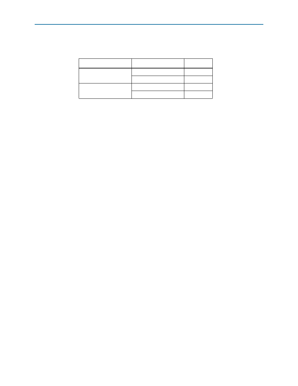
lists the VCCRT_GXB and VCCA_GXB voltage rails and their voltage level
depending on the switch position.
1
If the board is powered off and powered on again with SW2 in the open position, the
voltages for VCCRT_GXB and VCCA_GXB voltage rails read 0.90 V and 2.5 V respectively
and will not come up to the proper levels. This is due to the LTC2978 device trying to
adjust these rails to their programed values, which it cannot, due to the switch
position of SW2. The work around to this issue is to set switch SW2 in the close
position at power up.
The Clock Control
The Clock Control application allows you to set the four Si570 programmable
oscillators to any frequency between 10 MHz and 945 MHz and select frequencies to
1400 MHz.
The oscillator drives a 2-to-6 buffer that drives a copy of the clock to all four edges of
the FPGA.
The Clock Control application runs as a stand-alone application. ClockControl.exe
resides in the
On Windows, click Start > All Programs > Altera > Transceiver Signal Integrity
Development Kit, Stratix V GT Edition
<version> > Clock Control to start the
application.
f
For more information about the Si570 and the Stratix V GT development board’s
clocking circuitry and clock input pins, refer to the
Table 6–2. Voltage Level Setting
Switch (Position 1 and 2)
Schematic Net Name
Voltage (V)
Close (Default)
VCCRT_GXB
1.0
VCCA_GXB
3.0
Open
VCCRT_GXB
0.9
VCCA_GXB
2.5