Altera Transceiver Signal Integrity User Manual
Page 20
4–4
Chapter 4: Development Board Setup
Factory Default Switch Jumper Settings
Transceiver Signal Integrity Development Kit,
February 2013
Altera Corporation
Stratix V GT Edition User Guide
4. Set DIP switch bank (SW4) to match
5. Set DIP switch bank (SW5) to match
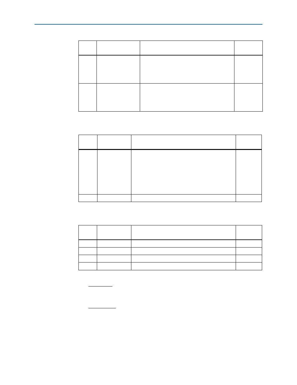
3
SW7-3 VCCT_GTB
Switch 3 has the following sequence enable
options:
■
ON position = VCCT_GTB is enabled.
■
OFF position = VCCT_GTB is disabled.
ON
4
SW7-4 VCCL_GTB
Switch 4 has the following sequence enable
options:
■
ON position = VCCL_GTB is enabled.
■
OFF position = VCCL_GTB is disabled.
ON
Table 4–4. SW4 User DIP Switch Settings
Switch
Board
Label
Function
Default
Position
1
S5_UNLOCK
Switch 1 has the following options:
■
Closed (0) = FACTORY command won’t be issued.
JTAG will be locked out if FPGA is configured on
power-up from flash.
■
Open (1) = Unlock the FPGA and allow FACTORY
command. JTAG will be available even if FPGA is
configured on power-up from flash.
Open (1)
2–8
DPI6—DPI0
User defined options.
—
Table 4–5. SW5 DIP Switch Settings
Switch
Board
Label
Function
Default
Position
1
S0
Determines S5GT_CLK11 frequency.
Closed
2
S1
Determines S5GT_CLK11 frequency.
Open
3
SS0
Determines S5GT_CLK11 spectrum spread.
Open
4
SS1
Determines S5GT_CLK11 spectrum spread.
Open
(1) Truth tables for the SW5 settings:
S1S0Frequency
00-25 MHz
01-100 MHz (default)
10-125 MHz
11-200 MHz
SS1SS0Spread %
00-center =/- 25%
01-down -0.5%
10-down -0.75%
11-no spread (default)
Table 4–3. SW7 DIP Switch Settings
Switch
Board
Label
Function
Default
Position