6 k1/k2 pin assignments: simultaneous start/ stop, K1/k2 pin assignments: simultaneous start/stop, Table 2-2: k1/k2 pin assignments – ADLINK PCI-8158 User Manual
Page 24: 14 installation, Table 2-1: p1/p2 pin assignments
14
Installation
X
P1 is for Axis 0 to 3 control and P2 is for Axis 4 to 7 control.
2.6 K1/K2 Pin Assignments: Simultaneous Start/
Stop
K1 and K2 are for simultaneous start/stop signals for multiple axes
or multiple cards.
Note: +5V and GND pins are provided by the PCI Bus power.
35
EZ1+
I
Encoder Z-phase (+)
85
EZ3+
I
Encoder Z-phase (+)
36
EZ1-
I
Encoder Z-phase (-)
86
EZ3-
I
Encoder Z-phase (-)
37
PEL0
I
End limit signal (+)
87
PEL2
I
End limit signal (+)
38
MEL0
I
End limit signal (-)
88
MEL2
I
End limit signal (-)
39
GDI0
I
DI/LTC/PCS/SD/CLR0
89
GDI2
I
DI/LTC/PCS/SD/CLR2
40
DO0
O
General Output 0
90
DO2
O
General Output 2
41
ORG0
I
Origin signal
91
ORG2
I
Origin signal
42
EXGND
Ext. power ground
92
EXGND
Ext. power ground
43
PEL1
I
End limit signal (+)
93
PEL3
I
End limit signal (+)
44
MEL1
I
End limit signal (-)
94
MEL3
I
End limit signal (-)
45
GDI1
I
DI/LTC/PCS/SD/CLR1/EMG
95
GDI3
I
DI/LTC/PCS/SD/CLR3
46
DO1
O
General Output 1
96
DO3
O
General Output 3
47
ORG1
I
Origin signal
97
ORG3
I
Origin signal
48
EXGND
-
Ext. power ground
98
EXGND
-
Ext. power ground
49
EXGND
-
Ext. power ground
99
E_24V
-
Isolation power Input, +24V
50
EXGND
-
Ext. power ground
100
E_24V
-
Isolation power Input, +24V
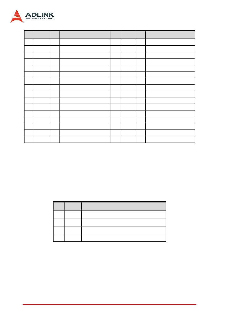
No. Name
Function
1
+5V
PCI Bus power Output (VCC)
2
STA
Simultaneous start signal input/output
3
STP
Simultaneous stop signal input/output
4
GND
PCI Bus power ground
Table 2-2: K1/K2 Pin Assignments
No.
Name
I/O
Function
No.
Name
I/O
Function
Table 2-1: P1/P2 Pin Assignments