Flash memory, Spartan-6 ddr2 – Digilent 410-178P-KIT User Manual
Page 11
Atlys Reference Manual
www.digilentinc.com
page 11 of 22
Copyright Digilent, Inc. All rights reserved. Other product and company names mentioned may be trademarks of their respective owners.
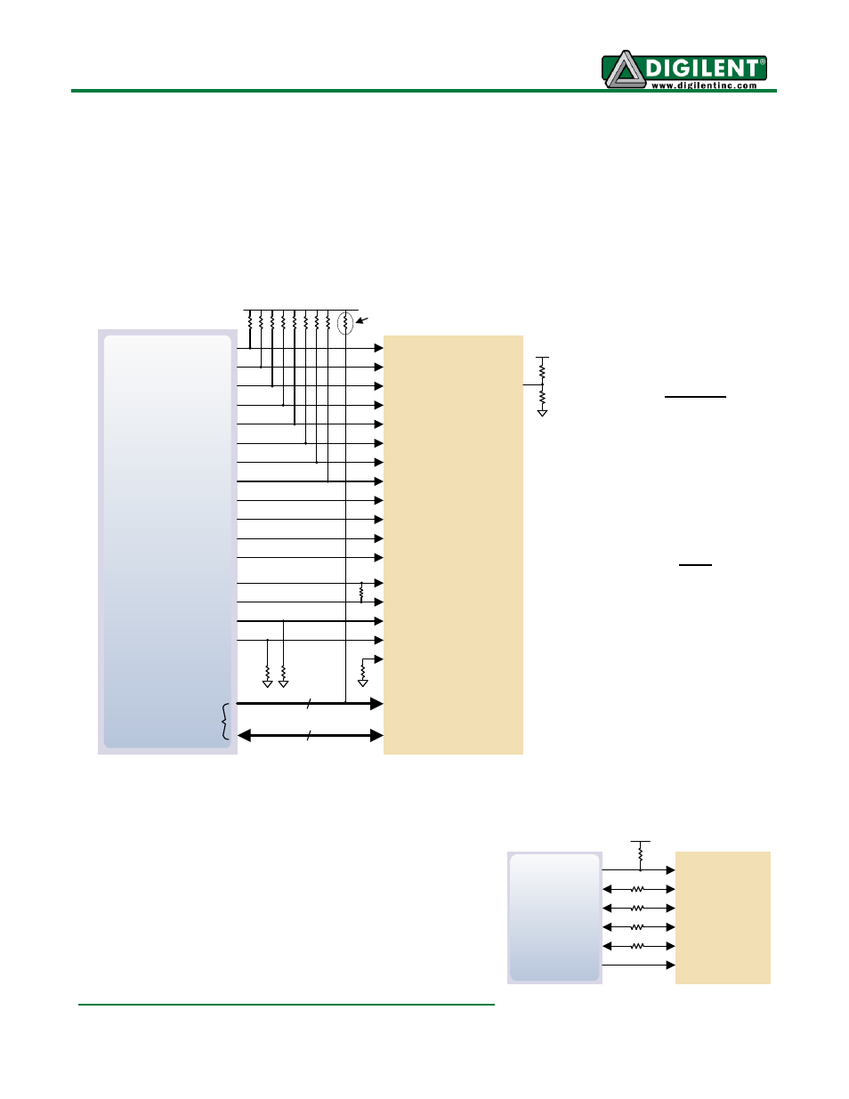
and control signals are delay-matched and impedance-controlled. Address and control signals are
terminated through 47-ohm resistors to a 0.9V V
TT
, and data signals use the On-Die-Termination
(ODT) feature of the DDR2 chip. Two well-matched DDR2 clock signal pairs are provided so the DDR
can be driven with low-skew clocks from the FPGA.
When generating a MIG core
for the MIRA part, selecting the “EDE1116AXXX-8E” device will result in
the correct timing parameters being set. When generating a component for the Micron part, it can be
selected by name within the wizard. The part loaded on your Atlys can be determined by examining
the print on the DDR2 component (IC13).
Flash Memory
The Atlys board uses a128Mbit Numonyx N25Q12 Serial
Flash memory device (organized as 16-bit by 16Mbytes) for
non-volatile storage of FPGA configuration files. The SPI
Flash can be programmed with a .bit, .bin., or .mcs file
using the Adept software. An FPGA configuration file
requires less than 12Mbits, leaving 116Mbits available for
user data. Data can be transferred from a PC to/from the
Flash by user applications, or by facilities built into the
Adept software. User designs programmed into the FPGA
can also transfer data to and from the ROM. A reference
Address
A12: G6
A4: F3
A11: D3
A3: L7
A10: F4
A2: H5
A9: D1
A1: J6
A8: D2
A0: J7
A7: H6
A6: H3
A5: H4
Data
D15: U1
D7: J1
D14: U2
D6: J3
D13: T1
D5: H1
D12: T2
D4: H2
D11: N1
D3: K1
D10: N2
D2: K2
D9: M1
D1: L1
D8: M3
D0: L2
DQ[15:0]
13
16
AD[12:0]
RAS#
CAS#
WE#
BA0
BA1
BA2
See Table
CS#
L4
P1
P2
E1
F1
F2
E3
K5
L5
Spartan-6
DDR2
x14
VREF
CKE
CK
CK#
UDQS_P
UDQS_N
LDQS_P
LDQS_N
UDM
LDM
ODT
1V8
L3
K4
K3
K6
H7
G1
G3
CS#
SDI/DQ0
SDO/DQ1
AH18
AF20
AF14
AE14
Spartan-6
SPI Flash
WP#/DQ2
HLD#/DQ3
AG21
AG17
SCK