Ddr2 memory – Digilent 410-178P-KIT User Manual
Page 10
Atlys Reference Manual
www.digilentinc.com
page 10 of 22
Copyright Digilent, Inc. All rights reserved. Other product and company names mentioned may be trademarks of their respective owners.
Power
Jack
Battery
Connector
Power Select
Jumper JP13
VU
1.8V
1.2V
2.5V
3.3V
IC16
IC15
IC16
IC15
EN
Power
Switch
Vswt
IC17
EN
0.9V
.01
Ω
LTC2481
To Digilent
Adept USB
I2C Bus
IC14
To Expansion
Connectors,
HDMI, USB
PG
PG
PG
PG
EN
EN
EN
Power On
LED (LD15)
LT3501
3A Regulator
LTC3546
1A Regulator
LT3501
3A Regulator
LTC3546
3A Regulator
ON
OFF
LTC3413
DDR Term. Reg.
Load Switch
J12
.01
Ω
LTC2481
.01
Ω
LTC2481
.01
Ω
LTC2481
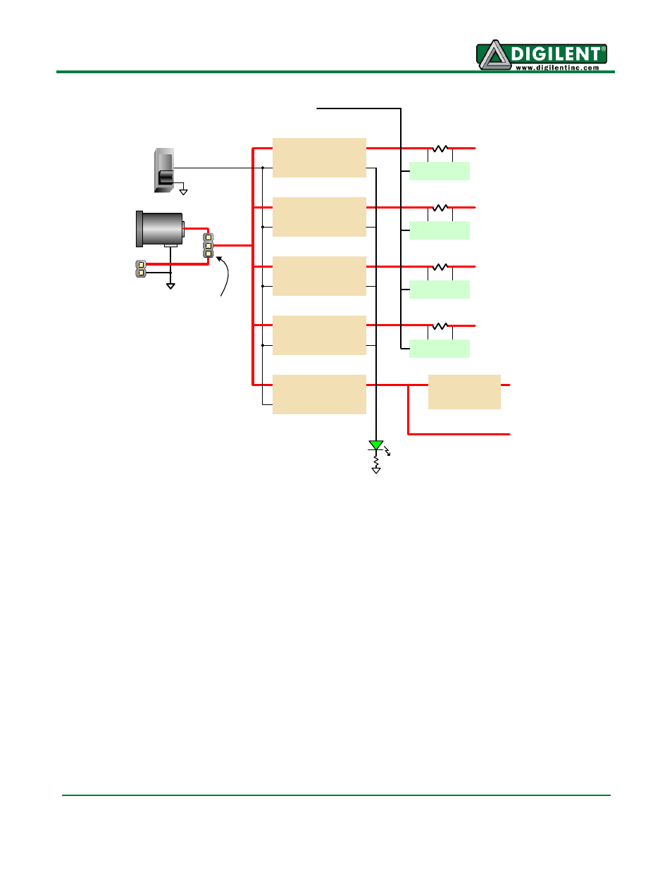
Atlys power supplies are enabled by a logic-level switch (SW8). A power-good LED (LD15), driven by
the wired-OR of all the power-good outputs on the supplies, indicates that all supplies are operating
within 10% of nominal.
A load switch (the FDC6330 at IC17) passes the input voltage VU to the Vswt node whenever the
power switch (SW8) is enabled. Vswt is assumed to be 5V, and is used by many systems on the
board including the HDMI ports, I2C bus, and USB host. Vswt is also available at expansion
connectors, so that any connected boards can be turned off along with the Atlys board.
DDR2 Memory
A single 1Gbit DDR2 memory chip is driven from the memory controller block in the Spartan-6 FGPA.
Previous versions of the Atlys were loaded with a Micron MT47H64M16-25E DDR2 component,
however, newly manufactured Atlys boards now carry an MIRA P3R1GE3EGF G8E DDR2
component. The datasheet for the MIRA device can be found be performing an internet search for
P3R1GE3JGF, which is an equivalent part. Both of these chips provide a 16-bit data bus and 64M
locations and have been tested for DDR2 operation at up to an 800MHz data rate.
The DDR2 interface follows the pinout and routing guidelines specified in the Xilinx Memory Interface
Generator (MIG) User Guide. The interface supports SSTL18 signaling, and all address, data, clocks,