Digilent 410-279P-KIT User Manual
Page 6
ZYBO™ FPGA Board Reference Manual
Copyright Digilent, Inc. All rights reserved.
Other product and company names mentioned may be trademarks of their respective owners.
Page 6 of 26
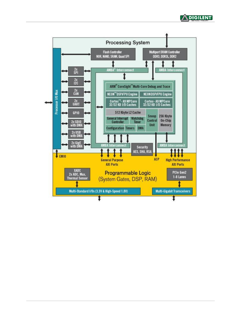
Figure 3. Zynq AP SoC architecture.
The PL is nearly identical to a Xilinx 7-series Artix FPGA, except that it contains several dedicated ports and buses
that tightly couple it to the PS. The PL also does not contain the same configuration hardware as a typical 7-series
FPGA, and it must be configured either directly by the processor or via the JTAG port.
The PS consists of many components, including the Application Processing Unit (APU, which includes 2 Cortex-A9
processors), Advanced Microcontroller Bus Architecture (AMBA) Interconnect, DDR3 Memory controller, and
various peripheral controllers with their inputs and outputs multiplexed to 54 dedicated pins (called
MultiplexedI/O, or MIO pins). Peripheral controllers that do not have their inputs and outputs connected to MIO
pins can instead route their I/O through the PL, via the Extended-MIO (EMIO) interface. The peripheral controllers
are connected to the processors as slaves via the AMBA interconnect, and contain readable/writable control
registers that are addressable in the processors’ memory space. The programmable logic is also connected to the
interconnect as a slave, and designs can implement multiple cores in the FPGA fabric that each also contain
addressable control registers. Furthermore, cores implemented in the PL can trigger interrupts to the processors
(connections not shown in Fig. 3) and perform DMA accesses to DDR3 memory.