11 vga port, Zybo™ fpga board reference manual – Digilent 410-279P-KIT User Manual
Page 17

ZYBO™ FPGA Board Reference Manual
Copyright Digilent, Inc. All rights reserved.
Other product and company names mentioned may be trademarks of their respective owners.
Page 17 of 26
When operating as Sink, the DDC function is required to be implemented so that a connected Source can read out
important characteristics of the device. This can be done by emulating an I
2
C-capable EEPROM in programmable
logic. Likewise, in Source mode DDC can be used to find out the capabilities of the connected display.
The HDMI/DVI protocol uses TMDS (Transition-minimized differential signaling) as I/O standard. It is supported on
Zynq by the I/O buffers on the programmable logic side. 50 ohm external parallel termination resistors are
provided on-board. HDMI specifications only require terminations on the Sink side, but optional Source-side
terminations reduce reflections, resulting in improved signal quality. Do not connect powered HDMI/DVI devices to
an unpowered ZYBO, as it might result in back-powering the board through the termination resistors.
Resolutions up to 720p (1280x720) have been tested.
HDMI and DVI are high-speed source-synchronous serial protocols. Implementations on FPGA are required to use
certain built-in primitives to properly synthesize the correct clock frequency, serialize the transmission, and keep a
lock on the signal. The actual implementation of the HDMI/DVI protocols is outside the scope of this manual.
Check for upcoming reference projects on our website or consult relevant specifications and Xilinx documentation.
11 VGA Port
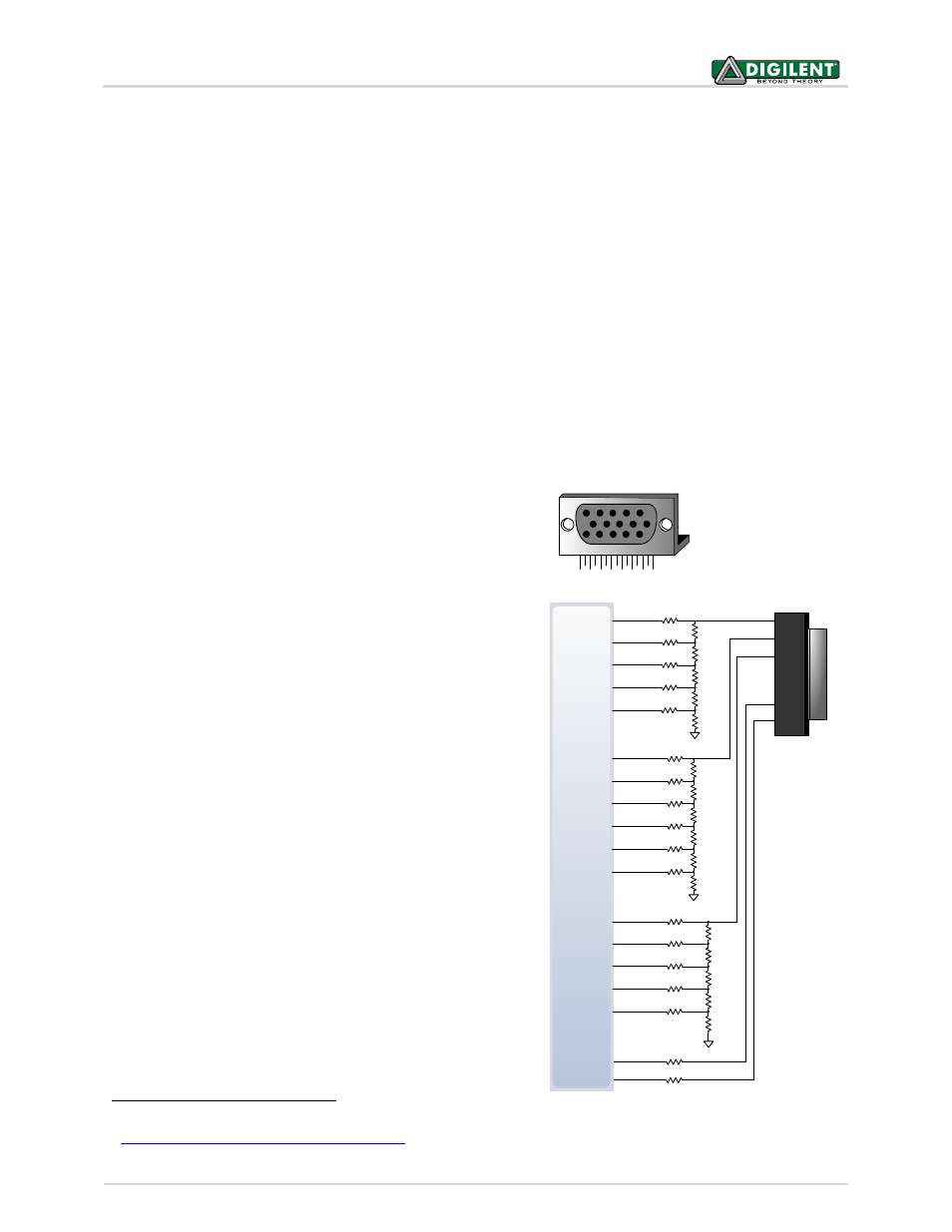
The ZYBO board uses 18 programmable logic pins to create an
analog VGA output port. This translates to 16-bit color depth and
two standard sync signals (HS – Horizontal Sync, and VS – Vertical
Sync).
The digital-to-analog conversion is done using a simple R-2R
resistor ladder
2
. The ladder works in conjunction with the 75-ohm
termination resistance of the VGA display to create 32 and 64
analog signal levels red, blue, and green VGA signals. This circuit,
shown in Fig. 8, produces video color signals that proceed in equal
increments between 0V (fully off) and 0.7V (fully on). With 5 bits
each for red and blue and 6 bits for green, 65,536 (32Ч32Ч64)
different colors can be displayed, one for each unique 16-bit
pattern.
A video controller circuit must be created in programmable logic
to drive the sync and color signals with the correct timing in order
to produce a working display system
Figure 8. ZYBO VGA circuit.
15
10
5
11
6
1
Pin 1: Red
Pin 2: Grn
Pin 3: Blue
Pin 13: HS
Pin 14: VS
Pin 5: GND
Pin 6: Red GND
Pin 7: Grn GND
Pin 8: Blu GND
Pin 10: Sync GND
HD-DB15F
100
W
100
W
RED5
RED4
RED3
RED
GRN
BLU
HS
VS
Zynq- 7
F19
G20
J20
P19
F20
H20
J19
R19
HSYNC
VSYNC
536
W
RED2
L20
L19
J18
K19
M20
P20
M19
N20
H18
G19
536
W
RED1
536
W
536
W
536
W
270
W
270
W
270
W
270
W
GRN5
GRN4
GRN3
536
W
GRN2
536
W
GRN1
536
W
536
W
536
W
270
W
270
W
270
W
270
W
536
W
GRN0
270
W
536
W
536
W
BLU5
BLU4
BLU3
536
W
BLU2
536
W
BLU1
536
W
536
W
536
W
270
W
270
W
270
W
270
W
536
W
