Pin description, Clock generator, Control pins and serial data i/o – Cirrus Logic CS5467 User Manual
Page 6: Analog inputs/outputs, Power supply connections, Cs5467
CS5467
6
DS714F3
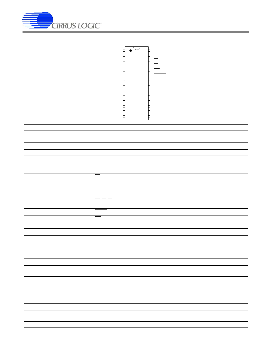
2. PIN DESCRIPTION
Clock Generator
Crystal Out
Crystal In
1,28
XOUT, XIN — Connect to an external quartz crystal. Alternatively, an external clock can be sup-
plied to the XIN pin to provide the system clock for the device.
CPU Clock Output
2
CPUCLK — Logic-level output from crystal oscillator. Can be used to clock an external CPU.
Control Pins and Serial Data I/O
Serial Clock
5
SCLK — Clocks serial data from the SDI pin and to the SDO pin when CS is low. SCLK is a
Schmitt-trigger input when MODE is low and a driven output when MODE is high.
Serial Data Output
6
SDO — Serial data output. Data is clocked out by SCLK.
Chip Select
7
CS — An input that enables the serial interface when MODE is low and a driven output when
MODE is high.
Mode Select
8
MODE — High selects external E
2
PROM, Low selects external microcontroller. MODE includes a
weak internal pull-down and therefore selects microcontroller mode if not connected.
Energy Output
22, 25,
26
E3, E1, E2 — Primarily active-low energy pulse outputs. These can be programmed to output
other conditions.
Reset
23
RESET — An active-low Schmitt-trigger input used to reset the chip.
Interrupt
24
INT — Active-low output, indicates that an enabled condition has occurred.
Serial Data Input
27
SDI — Serial data input. Data is clocked in by SCLK.
Analog Inputs/Outputs
Differential Voltage Inputs
9,10
13, 14
VIN1+, VIN1-, VIN2+, VIN2- — Differential analog inputs for the voltage channels.
Differential Current Inputs
20,19,
16,15
IIN1+, IIN1-, IIN2+, IIN2- — Differential analog inputs for the current channels.
Voltage Reference Output
11
VREFOUT — The on-chip voltage reference output. Nominally 2.5 V, referenced to AGND.
Voltage Reference Input
12
VREFIN — The voltage reference input. Can be connected to VREFOUT or external 2.5 V refer-
ence.
Power Supply Connections
Positive Digital Supply
3
VD+ — The positive digital supply.
Digital Ground
4
DGND — Digital ground.
Positive Analog Supply
18
VA+ — The positive analog supply.
Analog Ground
17
AGND — Analog ground.
Power Fail Monitor
21
PFMON — Used to monitor the unregulated power supply via a resistive divider. If the PFMON
voltage drops below its low limit, the low-supply detect (LSD) bit is set in the Status register.
VREFIN
12
Voltage Reference Input
VREFOUT
11
Voltage Reference Output
VIN1-
10
Differential Voltage Input
VIN1+
9
Differential Voltage Input
MODE
8
Mode Select
CS
7
Chip Select
SDO
6
Serial Data Ouput
SCLK
5
Serial Clock
DGND
4
Digital Ground
VD+
3
Positive Digital Supply
CPUCLK
2
CPU Clock Output
XOUT
1
Crystal Out
AGND
17
Analog Ground
VA+
18
Positive Analog Supply
IIN1-
19
Differential Current Input
IIN1+
20
Differential Current Input
PFMON
21
Power Fail Monitor
E3
22
Energy Output 3
RESET
23
Reset
INT
24
Interrupt
E1
25
Energy Output 1
26
SDI
27
Serial Data Input
XIN
28
Crystal In
E2
Energy Output 2
VIN2-
14
Differential Voltage Input
VIN2+
13
Differential Voltage Input
IIN2-
15
Differential Current Input
IIN2+
16
Differential Current Input