Signal path description, 1 analog-to-digital converters, 2 decimation filters – Cirrus Logic CS5467 User Manual
Page 14: 3 phase compensation, Cs5467
CS5467
14
DS714F3
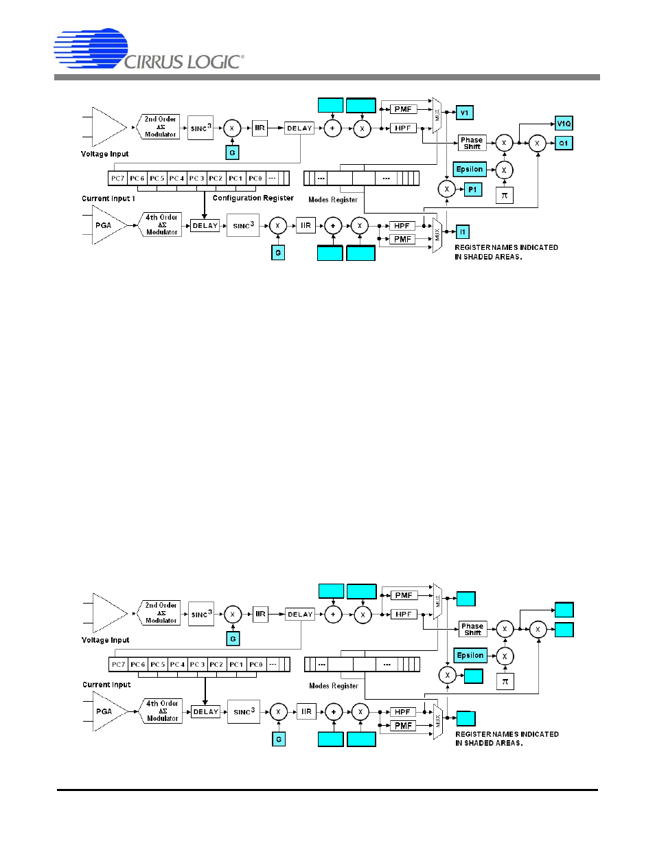
4. SIGNAL PATH DESCRIPTION
The data flow for voltage and current measurement and
the other calculations are shown in Figures
,
, and
.
4.1 Analog-to-Digital Converters
Voltage1 channel and voltage2/temperature channel
use second-order delta-sigma modulators and the two
current channels use fourth-order delta-sigma modula-
tors to convert the analog inputs to single-bit digital data
streams. The converters sample at a rate of DCLK/8.
This high sampling provides a wide dynamic range and
simplifies anti-alias filter design.
4.2 Decimation Filters
The single-bit modulator output data is widened to 24
bits and down-sampled to DCLK/1024 with low-pass
decimation filters. These decimation filters are third-or-
der Sinc. Their outputs are passed through third-order
IIR “anti-sinc” filters, used to compensate for the ampli-
tude roll-off of the decimation filters.
4.3 Phase Compensation
Phase compensation changes the phase of current rel-
ative to voltage by changing the sampling time in the
decimation filters. The amount of phase shift is set by
bits PC[7:0] in the Configuration register (Config) for
channel 1 and bits PC[7:0] in the Control register (Ctrl)
for channel 2.
Phase compensation, PC[7:0] is a signed two’s comple-
ment binary value in the range of -1.0 to almost +1.0
output word rate (OWR) samples. For a sample rate of
4000 Hz, the delay range is ±250 uS, a phase shift of
±4.5° at 50 Hz and ±5.4° at 60 Hz. The step size would
be 0.0352° at 50 Hz and 0.0422° at 60 Hz at this sample
rate.
Figure 3. Signal Flow for V1, I1, P1, Q1 Measurements
FGA
1
VHPF1 IHPF1
V1
GAIN
V1
OFF
I1
GAIN
I1
OFF
Figure 4. Signal Flow for V2, I2, P2, Q2 Measurements
FGA
2
2
V2Q
Q2
P2
V2
V2
GAIN
V2
OFF
I2
I2
GAIN
I2
OFF
Control Register
VHPF2 IHPF2