Cirrus Logic CS5467 User Manual
Cs5467 four-channel power/energy ic, Features & description, Description
Copyright
Cirrus Logic, Inc. 2011
(All Rights Reserved)
CS5467
Four-channel Power/Energy IC
Features
& Description
• Energy Linearity: ±0.1% of Reading over 1000:1
Dynamic Range
• On-chip Functions:
- Voltage and Current Measurement
- Active, Reactive, and Apparent Power/Energy
- RMS Voltage and Current Calculations
- Current Fault and Voltage Sag Detection
- Calibration
- Phase Compensation
- Temperature Sensor
- Energy Pulse Outputs
• Meets Accuracy Spec for IEC, ANSI, & JIS
• Low Power Consumption
• Voltage Tamper Correction
• Ground-referenced Inputs with Single Supply
• On-chip 2.5 V Reference (40 ppm / °C typ.)
• Power Supply Monitor Function
• Three-wire Serial Interface to Microcontroller or
E
2
PROM
• Power Supply Configurations
GND: 0 V, VA+: +5 V, VD+: +3.3 V to +5 V
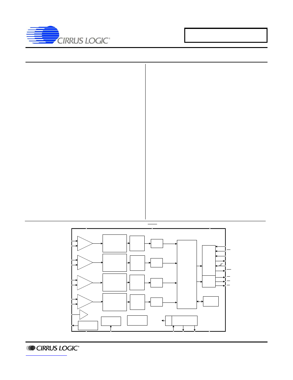
Description
The CS5467 is a watt-hour meter on a chip. It
measures line voltage and current and calcu-
lates active, reactive, apparent power, energy,
power factor, and RMS voltage and current.
An internal RMS voltage reference can be used
if voltage measurement is disabled by
tampering.
Four
analog-to-digital converters are used to
measure two voltages and two currents. Option-
ally, voltage2 channel can be used for
temperature measurement.
The CS5467 is designed to interface to a variety
of voltage and current sensors.
Additional features include system-level calibra-
tion, voltage sag and current fault detection,
peak detection, phase compensation, and ener-
gy pulse outputs.
ORDERING INFORMATION
See
VA+
VD+
IIN1+
IIN1-
VIN2+
VIN2-
VREFIN
VREFOUT
AGND
XIN
XOUT CPUCLK
DGND
CS
SDO
SDI
SCLK
INT
Voltage
Reference
System
Clock
/K
Clock
Generator
Serial
Interface
E-to-F
Power
Monitor
PFMON
x1
RESET
Digital
Filter
Calibration
MODE
Power
Calculation
Engine
4th Order
Modulator
2nd Order
Modulator
Temperature
Sensor
Digital
Filter
PGA
HPF
Option
HPF
Option
E1
E2
E3
x10
IIN2+
IIN2-
4th Order
Modulator
Digital
Filter
PGA
HPF
Option
VIN1+
VIIN1-
Digital
Filter
2nd Order
Modulator
HPF
Option
x10
JAN ‘11
DS714F3
Document Outline
- Features & Description
- 1. Overview
- 2. Pin Description
- 3. Characteristics & Specifications
- 4. Signal Path Description
- 5. Pin Descriptions
- 6. Setting Up the CS5467
- 6.1 Clock Divider
- 6.2 CPU Clock Inversion
- 6.3 Interrupt Pin Behavior
- 6.4 Current Input Gain Ranges
- 6.5 High-pass Filters
- 6.6 Cycle Count
- 6.7 Energy Pulse Outputs
- 6.8 No Load Threshold
- 6.9 Energy Pulse Width
- 6.10 Energy Pulse Rate
- 6.11 Voltage Sag/Current Fault Detection
- 6.12 Epsilon
- 6.13 Temperature Measurement
- 7. Using the CS5467
- 8. Register Descriptions
- 8.1 Page Register
- 8.2 Page 0 Registers
- 8.2.1 Configuration (Config) – Address: 0
- 8.2.2 Instantaneous Current (I1, I2), Voltage (V1, V2), and Power (P1, P2)
- 8.2.3 Active Power (P1AVG , P2AVG )
- 8.2.4 RMS Current (I1RMS , I2RMS ) and Voltage (V1RMS , V2RMS )
- 8.2.5 Instantaneous Quadrature Power (Q1, Q2)
- 8.2.6 Reactive Power (Q1Avg , Q2AVG )
- 8.2.7 Peak Current (I1PEAK, I2PEAK ) and Peak Voltage (V1PEAK, V2PEAK )
- 8.2.8 Apparent Power (S1, S2)
- 8.2.9 Power Factor (PF1, PF2)
- 8.2.10 Temperature (T) – Address: 27
- 8.2.11 Active, Apparent, and Reactive Energy Pulse Outputs (EPULSE , SPULSE , QPULSE )
- 8.2.12 Internal Status (Status) and Interrupt Mask (Mask)
- 8.2.13 Control (Ctrl) – Address: 28
- 8.3 Page 1 Registers
- 8.3.1 DC Offset for Current (I1OFF , I2OFF ) and Voltage (V1OFF , V2OFF )
- 8.3.2 Gain for Current (I1GAIN , I2GAIN ) and Voltage (V1GAIN , V2GAIN )
- 8.3.3 Power Offset (P1OFF , P2OFF )
- 8.3.4 AC Offset for Current (I1ACOFF , I2ACOFF ) and Voltage (V1ACOFF , V2ACOFF )
- 8.3.5 Mode Control (Modes) – Address: 16
- 8.3.6 Line to Sample Frequency Ratio (Epsilon) – Address: 17
- 8.3.7 Pulse Output Width (PulseWidth) – Address: 14
- 8.3.8 Pulse Output Rate (PulseRate) – Address: 15
- 8.3.9 Cycle Count (N) – Address: 19
- 8.3.10 Wideband Reactive Power (Q1WB , Q2WB )
- 8.3.11 Temperature Gain (TGAIN ) – Address: 22
- 8.3.12 Temperature Offset (TOFF ) – Address: 23
- 8.3.13 Filter Settling Time for Conversion Startup (TSETTLE ) – Address: 25
- 8.3.14 No Load Threshold (LoadMIN ) – Address: 26
- 8.3.15 Voltage Fixed RMS Reference (VFRMS ) – Address 27
- 8.3.16 System Gain (G) – Address: 28
- 8.3.17 System Time (Time) – Address: 29
- 8.4 Page 2 Registers
- 8.5 Page 5 Register
- 9. System Calibration
- 10. E2PROM Operation
- 11. Basic Application Circuits
- 12. Package Dimensions
- 13. Ordering Information
- 14. Environmental, Manufacturing, & Handling Information
- 15. Revision History