Switching characteristics, Start-up, Serial port timing – Cirrus Logic CS5467 User Manual
Page 11: Sdi timing, Sdo timing, E2prom mode timing, Cs5467
CS5467
DS714F3
11
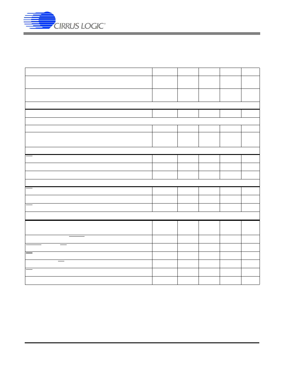
SWITCHING CHARACTERISTICS
• Min / Max characteristics and specifications are guaranteed over all
Recommended Operating Conditions
• Typical characteristics and specifications are measured at nominal supply voltages and TA = 25 °C.
• VA+ = 5 V ±5% VD+ = 3.3 V ±5% or 5 V ±5%; AGND = DGND = 0 V. All voltages with respect to 0 V.
• Logic Levels: Logic 0 = 0 V, Logic 1 = VD+.
Notes: 17. Specified using 10% and 90% points on waveform of interest. Output loaded with 50 pF.
18. Oscillator start-up time varies with crystal parameters. This specification does not apply when using an
external clock source.
Parameter
Symbol Min Typ
Max
Unit
Rise Times
(Note 17)
Any Digital Output
t
rise
-
-
-
50
1.0
-
µs
ns
Fall Times
(Note 17)
Any Digital Output
t
fall
-
-
-
50
1.0
-
µs
ns
Start-up
Oscillator Start-up Time
XTAL = 4.096 MHz (Note
)
t
ost
-
60
-
ms
Serial Port Timing
Serial Clock Frequency
SCLK
-
-
2
MHz
Serial Clock
Pulse Width High
Pulse Width Low
t
1
t
2
200
200
-
-
-
-
ns
ns
SDI Timing
CS Falling to SCLK Rising
t
3
50
-
-
ns
Data Set-up Time Prior to SCLK Rising
t
4
50
-
-
ns
Data Hold Time After SCLK Rising
t
5
100
-
-
ns
SDO Timing
CS Falling to SDO Driving
t
6
-
20
50
ns
SCLK Falling to New Data Bit (hold time)
t
7
-
20
50
ns
CS Rising to SDO Hi-Z
t
8
-
20
50
ns
E
2
PROM mode Timing
Serial Clock
Pulse Width Low
Pulse Width High
t
9
t
10
8
8
DCLK
DCLK
MODE setup time to RESET Rising
t
11
50
ns
RESET rising to CS falling
t
12
48
DCLK
CS falling to SCLK rising
t
13
100
8
DCLK
SCLK falling to CS rising
t
14
16
DCLK
CS rising to driving MODE low
t
15
50
ns
SDO setup time to SCLK rising
t
16
100
ns