Setting up the cs5467, 1 clock divider, 2 cpu clock inversion – Cirrus Logic CS5467 User Manual
Page 20: 3 interrupt pin behavior, 4 current input gain ranges, 5 high-pass filters, 6 cycle count, 7 energy pulse outputs, Table 1. interrupt configuration, Table 2. current input gain ranges
CS5467
20
DS714F3
6. SETTING UP THE CS5467
6.1 Clock Divider
The internal clock to the CS5467 needs to operate
around 4 MHz. However, by using the internal clock di-
vider, a higher crystal frequency can be used. This is im-
portant when driving an external microcontroller
requiring a faster clock and using the CPUCLK output.
K is the divide ratio from the crystal input to the internal
clock and is selected with Configuration register (Con-
fig
) bits K[3:0]. It has a range of 1 to 16. A value of zero
results in a setting of 16.
6.2 CPU Clock Inversion
By default, CPUCLK is inverted from XIN. Setting Con-
figuration register bit iCPU removes this inversion. This
can be useful when one phase adds more noise to the
system than the other.
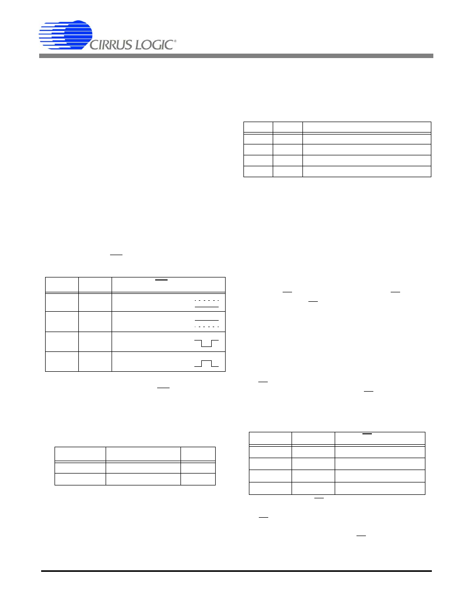
6.3 Interrupt Pin Behavior
The behavior of the INT pin is controlled by the IMODE
and IINV bits in the Configuration register as shown.
If IMODE = 1, the duration of the INT pulse will be two
DCLK cycles, where DCLK = MCLK/K.
6.4 Current Input Gain Ranges
Control register bits I1gain (I2gain) select the input
range of the current inputs.
6.5 High-pass Filters
Mode Control (Modes) register bits VHPF and IHPF ac-
tivate the HPF in the voltage and current paths, respec-
tively. Each energy channel has separate VHPF and
IHPF bits. When a high-pass filter is enabled in only one
path within a channel, a phase matching filter (PMF) is
applied to the other path within that channel. The PMF
filter matches the amplitude and phase response of the
HPF in the band of interest, but passes DC.
6.6 Cycle Count
Low-rate calculations, such as average power and RMS
voltage and current integrate over several (N) output
word rate (OWR) samples. The duration of this averag-
ing window is set by the Cycle Count (N) register. By de-
fault, Cycle Count is set to 4000 (1 second at output
word rate [OWR] of 4000 Hz). The minimum value for
Cycle Count is 10.
6.7 Energy Pulse Outputs
By default, E1 outputs total active energy, E3, total re-
active energy, and E2, the sign of both active and reac-
tive energy. (See
Figure 2. Timing Diagram for E1, E2,
Three pairs of bits in the Mode Control (Modes) register
control the operation of these outputs. These bits are
named E1MODE[1:0], E2MODE[1:0], and
E3MODE[1:0]. Some combinations of these bits over-
ride others, so read the following paragraphs carefully.
The E2 pin can output energy sign, or total apparent en-
ergy. Table 4 lists the functions of E2 as controlled by
E2MODE[1:0] in the Modes register.
Note: E2MODE[1:0]=3 is a special mode.
The E3 pin can output total reactive energy, power fail
monitor status, voltage1 sign, or total apparent energy.
Table 5 lists the functions of E3 as controlled by
IMODE
IINV
INT Pin
0
0
Active-low Level
0
1
Active-high Level
1
0
Low Pulse
1
1
High Pulse
Table 1. Interrupt Configuration
I1gain, I2gain
Maximum Input
Gain
0
±250 mV
10x
1
±50 mV
50x
Table 2. Current Input Gain Ranges
VHPF
IHPF
Filter Configuration
0
0
No filter on Voltage or Current
0
1
HPF on Current, PMF on Voltage
1
0
HPF on Voltage, PMF on Current
1
1
HPF on Current and Voltage
Table 3. High-pass Filter Configuration
E2MODE1 E2MODE0
E2 output
0
0
Energy Sign
0
1
Total Apparent Energy
1
0
Not Used
1
1
Enable E1MODE
Table 4. E2 Pin Configuration