Power supplies, 1 analog power supplies, 2 digital power supply – Cirrus Logic CS5374 User Manual
Page 32: 3 power supply bypassing, Analog power supplies, Digital power supply, Power supply bypassing, Figure 19. power supply diagram, Cs5374
CS5374
CS5374
32
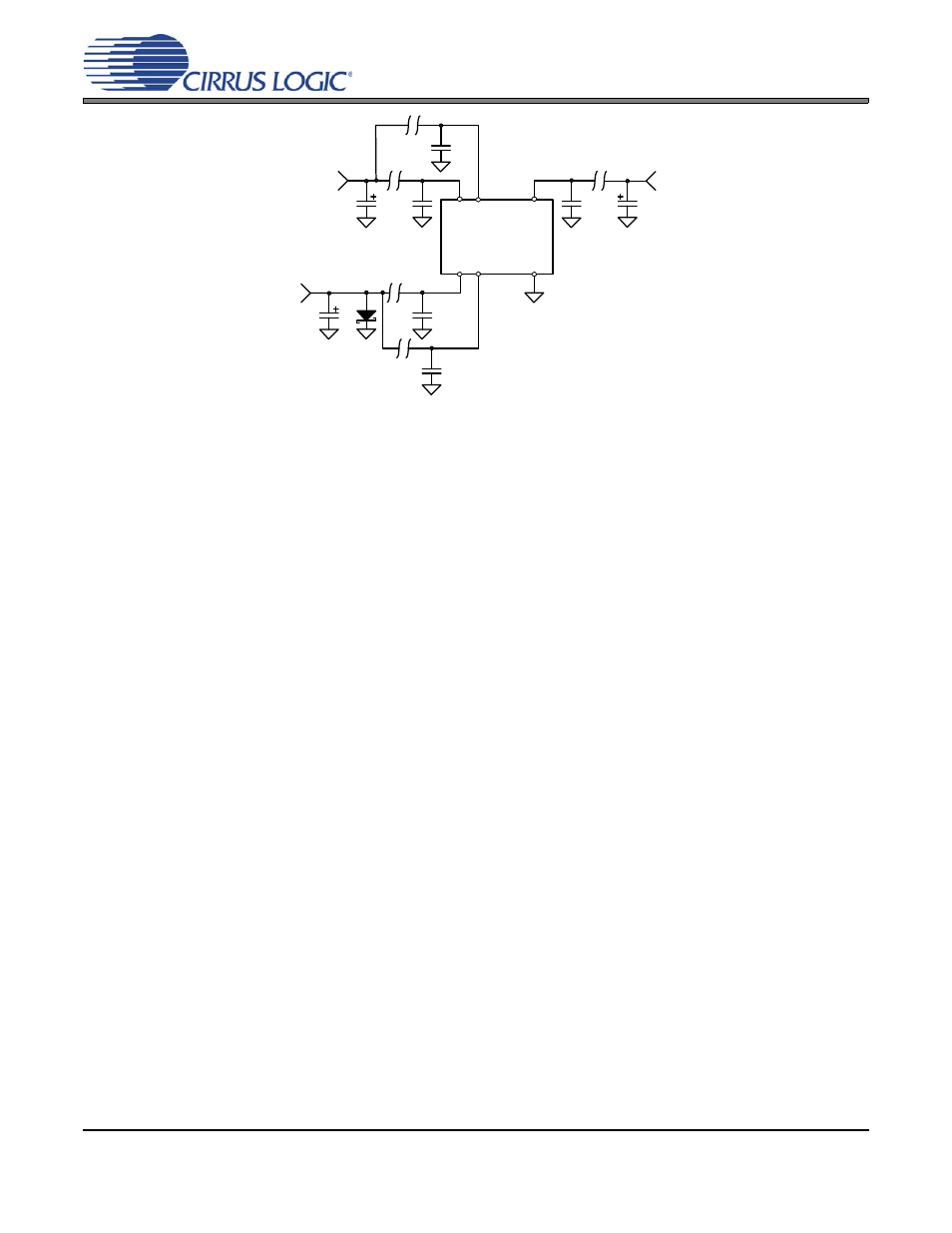
8. POWER SUPPLIES
The CS5374 has two positive analog power supply
pins (VA+), two negative analog power supply
pins (VA–), a digital power supply pin (VD+), and
a ground pin (GND).
For proper operation, power must be supplied to all
power supply pins, and the ground pin must be con-
nected to system ground. The CS5374 digital pow-
er supply (VD+) and the CS5376A digital power
supply (VD) must share a common voltage.
8.1 Analog Power Supplies
The analog power pins of the CS5374 are to be sup-
plied with a total of 5 V between VA+ and VA–
from a bipolar ±2.5 V supply. When using bipolar
supplies the analog signal common mode voltage
should be biased to 0 V. The analog power supplies
are recommended to be bypassed to system ground
using 0.1
μF X7R type capacitors.
The VA– supply is connected to the CMOS sub-
strate and as such must remain the most negative
applied voltage to prevent potential latch-up condi-
tions. It is recommended to clamp the VA– supply
to system ground using a reverse biased Schottky
diode to prevent possible latch-up conditions relat-
ed to mismatched supply rail initialization.
Care should be taken to connect the CS5374 ther-
mal pad on the bottom of the package to VA–, not
system ground (GND), since it internally connects
to VA– and is expected to be the most negative ap-
plied voltage.
8.2 Digital Power Supply
The digital power supply across the VD and GND
pins is specified for a +3.3 V power supply. The
digital power supply should be bypassed to system
ground using a 0.01
μF X7R type capacitor. The
digital power supply across the VD+ and GND pins
is specified to be +3.3 V.
8.3 Power Supply Bypassing
The VA+ and VA– power supplies should be by-
passed to system ground with 0.1
μF capacitors
placed as close as possible to the power pins of the
device. The VD+ power supply should be bypassed
to system ground with 0.1
μF capacitors placed as
close as possible to the power pins of the device.
Bypass capacitors should be X7R, C0G, tantalum,
or other high-quality dielectric type.
In addition to the local bypass capacitors, at least
100
μF bulk capacitance to system ground should
be placed on each power supply near the voltage
CS5374
VA+
VD+
VA-
GND
0.01 uF
100 uF
0.1 uF
100 uF
100 uF
0.1 uF
To VA+
Regulator
To VA-
Regulator
To VD
Regulator
VA+
VA-
0.1 uF
0.1 uF
Figure 19. Power Supply Diagram