Voltage reference, 1 vref power supply, 2 vref rc filter – Cirrus Logic CS5374 User Manual
Page 30: 3 vref pcb routing, 4 vref input impedance, Vref power supply, Vref rc filter, Vref pcb routing, Vref input impedance, Figure 18. voltage reference circuit
CS5374
CS5374
30
7.
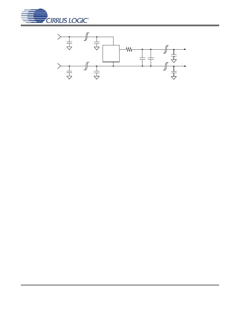
VOLTAGE REFERENCE
The CS5374 modulators require a 2.500 V preci-
sion voltage reference to be supplied to the VREF
±
pins.
7.1 VREF Power Supply
To guarantee proper regulation headroom for the
voltage reference device, the voltage reference
GND pin should be connected to VA– instead of
system ground, as shown in
nection results in a VREF– voltage equal to VA–
and a VREF+ voltage very near ground potential
[(VA–) + 2.500 VREF].
Power supply inputs to the voltage reference device
should be bypassed to system ground with 0.1
μF
capacitors placed as close as possible to the power
and ground pins. In addition to 0.1
μF local bypass
capacitors, at least 100
μF of bulk capacitance to
system ground should be placed on each power
supply near the voltage regulator outputs. Bypass
capacitors should be X7R, C0G, tantalum, or other
high-quality dielectric type.
7.2 VREF RC Filter
LT1019AIS8-2.5
voltage reference yields accept-
able noise levels if the output is filtered with a low-
pass RC filter.
A separate RC filter is required for each device
connected to the voltage reference output. Signal-
dependent sampling of the voltage reference by one
system device could cause unwanted tones to ap-
pear in the measurement bandwidth of another sys-
tem device if a single VREF RC filter is common
to both.
7.3 VREF PCB Routing
To minimize the possibility of outside noise cou-
pling into the CS5374 voltage reference input, the
VREF
±
traces should be routed as a differential
pair from the large capacitor of the voltage refer-
ence RC filter. Careful control of the voltage refer-
ence source and return currents by routing VREF
±
as a differential pair will significantly improve im-
munity from external noise.
To further improve noise rejection of the VREF
±
differential route,
include 0.1
μF
bypass
capaci-
tors to system ground as close as possible to the
VREF+ and VREF– pins of the CS5374.
7.4 VREF Input Impedance
The switched-capacitor input architecture of the
VREF
±
inputs results in an input impedance that
depends on the internal capacitor size and the
MCLK frequency. With a 15 pF internal capacitor
and a 2.048 MHz MCLK, the VREF input imped-
ance is approximately
10
Ω
To VREF+
+
From VA+
Regulator
2.500 V
VREF
0.1
μF
To VREF-
0.1
μF
100
μF
0.1
μF
0.1
μF
0.1
μF
100
μF
100
μF
From VA-
Regulator
Route VREF
± as a differential pair
from the 100uF RC filter capacitor
Figure 18. Voltage Reference Circuit